- 您現在的位置:買賣IC網 > PDF目錄382948 > ECP103G-PCB2450 (Electronic Theatre Controls, Inc.) 1 Watt, High Linearity InGaP HBT Amplifier PDF資料下載
參數資料
| 型號: | ECP103G-PCB2450 |
| 廠商: | Electronic Theatre Controls, Inc. |
| 英文描述: | 1 Watt, High Linearity InGaP HBT Amplifier |
| 中文描述: | 1瓦特,高線性InGaP HBT功率放大器 |
| 文件頁數: | 1/5頁 |
| 文件大小: | 382K |
| 代理商: | ECP103G-PCB2450 |
Specifications and information are subject to change without notice
WJ Communications, Inc
Phone 1-800-WJ1-4401 FAX: 408-577-6621 e-mail: sales@wj.com Web site: www.wj.com
October 2004 Rev 1
ECP103
1 Watt, High Linearity InGaP HBT Amplifier
Product Information
The Communications Edge
TM
Product Features
x
2300 - 2700 MHz
x
+30.5 dBm P1dB
x
+46 dBm Output IP3
x
10 dB Gain @ 2450 MHz
x
9 dB Gain @ 2600 MHz
x
Single Positive Supply (+5V)
x
Available in SOIC-8 or 16pin
4mm QFN package
Applications
x
W-LAN
x
RFID
x
DMB
x
Fixed Wireless
Specifications
(1)
Product Description
The ECP103 is a high dynamic range driver amplifier in
a low-cost surface mount package. The InGaP/GaAs
HBT is able to achieve superior performance for various
narrowband-tuned application circuits with up to +46
dBm OIP3 and +30.5 dBm of compressed 1-dB power.
The part is housed in an industry standard SOIC-8 SMT
package. All devices are 100% RF and DC tested.
The ECP103 is targeted for use as a driver amplifier in
wireless infrastructure where high linearity and medium
power is required. An internal active bias allows the
ECP103 to maintain high linearity over temperature and
operate directly off a single +5V supply. This
combination makes the device an excellent candidate for
driver amplifier stages in wireless-LAN, digital
multimedia broadcast, or fixed wireless applications. The
device can also be used in next generation RFID readers.
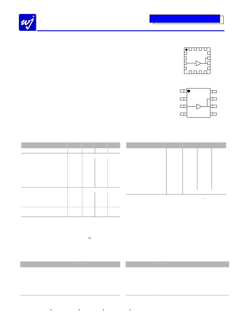
Functional Diagram
1
Vref
ECP103D
ECP103G
Parameter
Operational Bandwidth
Test Frequency
Gain
Input Return Loss
Output Return Loss
Output P1dB
Output IP3
Noise Figure
Test Frequency
Gain
Output P1dB
Output IP3
(2)
Operating Current Range , Icc
(3)
Device Voltage, Vcc
Units Min Typ Max
MHz
2300
MHz
dB
dB
dB
dBm
dBm
dB
MHz
dB
dBm
dBm
mA
400
V
2700
2450
10
18
8
+30.5
+46
6.3
2600
9
+30
+45
450
5
(2)
500
1. Test conditions unless otherwise noted:
T = 25oC, Vsupply = +5 V in a tuned application circuit.
2. 3OIP measured with two tones at an output power of +15 dBm/tone separated by 1 MHz. The
suppression on the largest IM3 product is used to calculate the 3OIP using a 2:1 rule.
3. This corresponds to the quiescent current or operating current under small-signal conditions into
pins 6, 7, and 8. It is expected that the current can increase by an additional 90 mA at P1dB. Pin 1
is used as a reference voltage for the internal biasing circuitry. It is expected that Pin 1 will pull
10.8 mA of current when used with a series bias resistor of R1=51 . (ie. total device current
typically will be 461 mA.)
Absolute Maximum Rating
Typical Performance
(4)
Parameter
Frequency
S21
– Gain
S11
S22
Output P1dB
Output IP3
W-CDMA Channel Power
@ -45 dBc ACPR
Noise Figure
Supply Bias
(3)
Units
MHz
dB
dB
dB
dBm
dBm
dBm
dB
Typical
7
+5 V @ 450 mA
2450
10
15
8
30.5
46
22.5
7
2600
9
15
8
30.0
45
7
4. Typical parameters reflect performance in a tuned application circuit at +25 C.
Ordering Information
Parameters
Operating Case Temperature
Storage Temperature
RF Input Power (continuous)
Device Voltage
Device Current
Device Power
Rating
-40 to +85
q
C
-65 to +150
q
C
+26 dBm
+8 V
900 mA
5 W
Part No.
ECP103D
ECP103G
ECP103D-PCB2450
ECP103D-PCB2650
ECP103G-PCB2450
ECP103G-PCB2650
Description
1 Watt InGaP HBT Amplifier (16p 4mm Pkg)
1 Watt InGaP HBT Amplifier (Soic-8 Pkg)
2450 MHz Evaluation Board
2600 MHz Evaluation Board
2450 MHz Evaluation Board
2600 MHz Evaluation Board
Operation of this device above any of these parameters may cause permanent damage.
2
3
4
12
11
10
9
16
15
14
13
5
6
7
N
8
N
N/C
RF OUT
RF OUT
N/C
N/C
RF IN
N/C
V
N
N
N
N
N
1
2
3
4
8
7
6
5
Vref
N/C
RF IN
N/C
Vbias
RF OUT
RF OUT
N/C
相關PDF資料 |
PDF描述 |
|---|---|
| ECP103G-PCB2650 | 1 Watt, High Linearity InGaP HBT Amplifier |
| ECP203D-PCB2450 | MB 8C 8#12 SKT PLUG |
| ECP203D-PCB2650 | 2 Watt, High Linearity InGaP HBT Amplifier |
| ECP203 | 2 Watt, High Linearity InGaP HBT Amplifier |
| ECP203D | 2 Watt, High Linearity InGaP HBT Amplifier |
相關代理商/技術參數 |
參數描述 |
|---|---|
| ECP103G-PCB2650 | 功能描述:射頻開發工具 2650MHz Eval Brd 10dB Gain RoHS:否 制造商:Taiyo Yuden 產品:Wireless Modules 類型:Wireless Audio 工具用于評估:WYSAAVDX7 頻率: 工作電源電壓:3.4 V to 5.5 V |
| ECP112 | 制造商:Apex Tool Group 功能描述:Crimp tool with die set for commercial open-barel; 22-10AWG |
| ECP12126 | 功能描述:機架和機柜配件 12X12X6 COMMAND RoHS:否 制造商:Bivar 產品:Rack Accessories 面板空間: 顏色:Black |
| ECP12168 | 功能描述:機架和機柜配件 HOLE PLUG STAINLESS RoHS:否 制造商:Bivar 產品:Rack Accessories 面板空間: 顏色:Black |
| ECP130PS12 | 功能描述:AC/DC CONVERTER 12V 100W 制造商:xp power 系列:ECP130 零件狀態:有效 類型:開放框架 輸出數:1 電壓 - 輸入:85 ~ 264 VAC 電壓 - 輸出 1:12V 電壓 - 輸出 2:- 電壓 - 輸出 3:- 電壓 - 輸出 4:- 電流 - 輸出(最大值):8.33A 功率(W):100W(130W 強制風冷) 應用:ITE(商業),醫療 電壓 - 隔離:4kV(4000V) 效率:93% 工作溫度:-20°C ~ 70°C(有降額) 特性:PFC,待機輸出,通用輸入 安裝類型:底座安裝 大小/尺寸:3.00" 長 x 2.00" 寬 x 1.10" 高(76.2mm x 50.8mm x 28.0mm) 所需最小負載:無 認可:CE 功率(W) - 最大值:100W (130W 強制風冷) 標準包裝:1 |
發布緊急采購,3分鐘左右您將得到回復。