- 您現(xiàn)在的位置:買賣IC網(wǎng) > PDF目錄22011 > EP1K100FC484-2 (Altera)IC ACEX 1K FPGA 100K 484-FBGA PDF資料下載
參數(shù)資料
| 型號: | EP1K100FC484-2 |
| 廠商: | Altera |
| 文件頁數(shù): | 8/86頁 |
| 文件大小: | 0K |
| 描述: | IC ACEX 1K FPGA 100K 484-FBGA |
| 產(chǎn)品培訓模塊: | Three Reasons to Use FPGA's in Industrial Designs |
| 標準包裝: | 60 |
| 系列: | ACEX-1K® |
| LAB/CLB數(shù): | 624 |
| 邏輯元件/單元數(shù): | 4992 |
| RAM 位總計: | 49152 |
| 輸入/輸出數(shù): | 333 |
| 門數(shù): | 257000 |
| 電源電壓: | 2.375 V ~ 2.625 V |
| 安裝類型: | 表面貼裝 |
| 工作溫度: | 0°C ~ 70°C |
| 封裝/外殼: | 484-BGA |
| 供應商設備封裝: | 484-FBGA(23x23) |
| 其它名稱: | 544-1061 |
第1頁第2頁第3頁第4頁第5頁第6頁第7頁當前第8頁第9頁第10頁第11頁第12頁第13頁第14頁第15頁第16頁第17頁第18頁第19頁第20頁第21頁第22頁第23頁第24頁第25頁第26頁第27頁第28頁第29頁第30頁第31頁第32頁第33頁第34頁第35頁第36頁第37頁第38頁第39頁第40頁第41頁第42頁第43頁第44頁第45頁第46頁第47頁第48頁第49頁第50頁第51頁第52頁第53頁第54頁第55頁第56頁第57頁第58頁第59頁第60頁第61頁第62頁第63頁第64頁第65頁第66頁第67頁第68頁第69頁第70頁第71頁第72頁第73頁第74頁第75頁第76頁第77頁第78頁第79頁第80頁第81頁第82頁第83頁第84頁第85頁第86頁
16
Altera Corporation
ACEX 1K Programmable Logic Device Family Data Sheet
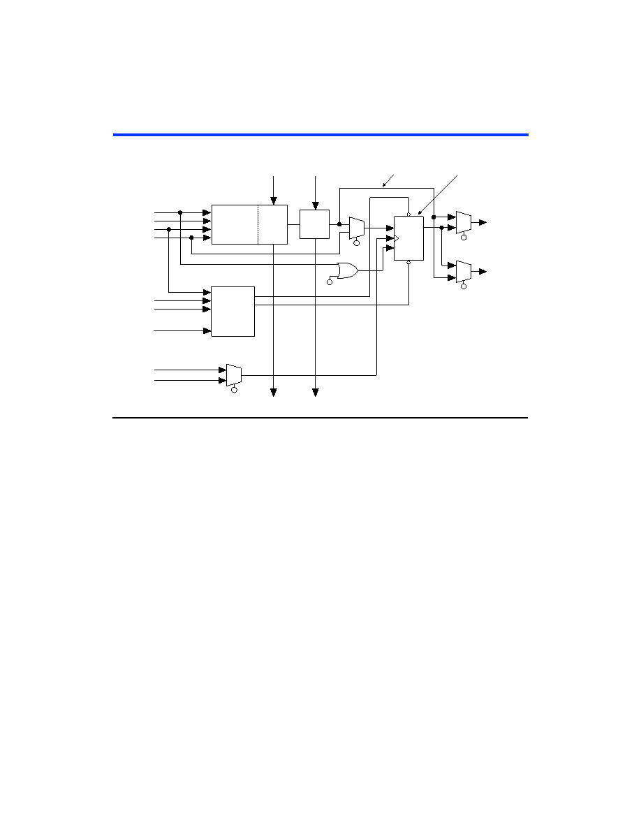
Figure 8. ACEX 1K Logic Element
The programmable flipflop in the LE can be configured for D, T, JK, or SR
operation. The clock, clear, and preset control signals on the flipflop can
be driven by global signals, general-purpose I/O pins, or any internal
logic. For combinatorial functions, the flipflop is bypassed and the LUT’s
output drives the LE’s output.
The LE has two outputs that drive the interconnect: one drives the local
interconnect, and the other drives either the row or column FastTrack
Interconnect routing structure. The two outputs can be controlled
independently. For example, the LUT can drive one output while the
register drives the other output. This feature, called register packing, can
improve LE utilization because the register and the LUT can be used for
unrelated functions.
The ACEX 1K architecture provides two types of dedicated high-speed
data paths that connect adjacent LEs without using local interconnect
paths: carry chains and cascade chains. The carry chain supports high-
speed counters and adders, and the cascade chain implements wide-input
functions with minimum delay. Carry and cascade chains connect all LEs
in a LAB and all LABs in the same row. Intensive use of carry and cascade
chains can reduce routing flexibility. Therefore, the use of these chains
should be limited to speed-critical portions of a design.
To LAB Local
Interconnect
Carry-In
Clock
Select
Carry-Out
Look-Up
Table
(LUT)
Clear/
Preset
Logic
Carry
Chain
Cascade
Chain
Cascade-In
Cascade-Out
To FastTrack
Interconnect
Programmable
Register
PRN
CLRN
DQ
ENA
Register Bypass
data1
data2
data3
data4
labctrl1
labctrl2
labctrl4
labctrl3
Chip-Wide
Reset
相關PDF資料 |
PDF描述 |
|---|---|
| D15P13F6GL00LF | CONN DSUB PLUG 15POS T/H RA GOLD |
| 2-1624113-4 | INDUCTOR 5.6NH 5% 0805 |
| VI-JNH-CW | CONVERTER MOD DC/DC 52V 100W |
| REC3-4815SRW/H/B/M | CONV DC/DC 3W 36-72VIN 15VOUT |
| 3-1624113-6 | INDUCTOR 33NH 5% 0805 |
相關代理商/技術參數(shù) |
參數(shù)描述 |
|---|---|
| EP1K100FC484-2N | 功能描述:FPGA - 現(xiàn)場可編程門陣列 FPGA - ACEX 1K 624 LABs 333 IOs RoHS:否 制造商:Altera Corporation 系列:Cyclone V E 柵極數(shù)量: 邏輯塊數(shù)量:943 內嵌式塊RAM - EBR:1956 kbit 輸入/輸出端數(shù)量:128 最大工作頻率:800 MHz 工作電源電壓:1.1 V 最大工作溫度:+ 70 C 安裝風格:SMD/SMT 封裝 / 箱體:FBGA-256 |
| EP1K100FC484-3 | 功能描述:FPGA - 現(xiàn)場可編程門陣列 FPGA - ACEX 1K 624 LABs 333 IOs RoHS:否 制造商:Altera Corporation 系列:Cyclone V E 柵極數(shù)量: 邏輯塊數(shù)量:943 內嵌式塊RAM - EBR:1956 kbit 輸入/輸出端數(shù)量:128 最大工作頻率:800 MHz 工作電源電壓:1.1 V 最大工作溫度:+ 70 C 安裝風格:SMD/SMT 封裝 / 箱體:FBGA-256 |
| EP1K100FC484-3N | 功能描述:FPGA - 現(xiàn)場可編程門陣列 FPGA - ACEX 1K 624 LABs 333 IOs RoHS:否 制造商:Altera Corporation 系列:Cyclone V E 柵極數(shù)量: 邏輯塊數(shù)量:943 內嵌式塊RAM - EBR:1956 kbit 輸入/輸出端數(shù)量:128 最大工作頻率:800 MHz 工作電源電壓:1.1 V 最大工作溫度:+ 70 C 安裝風格:SMD/SMT 封裝 / 箱體:FBGA-256 |
| EP1K100FI2562 | 制造商:Altera Corporation 功能描述: |
| EP1K100FI256-2 | 功能描述:FPGA - 現(xiàn)場可編程門陣列 FPGA - ACEX 1K 624 LABs 186 IOs RoHS:否 制造商:Altera Corporation 系列:Cyclone V E 柵極數(shù)量: 邏輯塊數(shù)量:943 內嵌式塊RAM - EBR:1956 kbit 輸入/輸出端數(shù)量:128 最大工作頻率:800 MHz 工作電源電壓:1.1 V 最大工作溫度:+ 70 C 安裝風格:SMD/SMT 封裝 / 箱體:FBGA-256 |
發(fā)布緊急采購,3分鐘左右您將得到回復。