- 您現在的位置:買賣IC網 > PDF目錄22011 > EP1K100FC484-2N (Altera)IC ACEX 1K FPGA 100K 484-FBGA PDF資料下載
參數資料
| 型號: | EP1K100FC484-2N |
| 廠商: | Altera |
| 文件頁數: | 46/86頁 |
| 文件大小: | 0K |
| 描述: | IC ACEX 1K FPGA 100K 484-FBGA |
| 產品培訓模塊: | Three Reasons to Use FPGA's in Industrial Designs |
| 標準包裝: | 60 |
| 系列: | ACEX-1K® |
| LAB/CLB數: | 624 |
| 邏輯元件/單元數: | 4992 |
| RAM 位總計: | 49152 |
| 輸入/輸出數: | 333 |
| 門數: | 257000 |
| 電源電壓: | 2.375 V ~ 2.625 V |
| 安裝類型: | 表面貼裝 |
| 工作溫度: | 0°C ~ 85°C |
| 封裝/外殼: | 484-BGA |
| 供應商設備封裝: | 484-FBGA(23x23) |
| 其它名稱: | 544-1822 EP1K100FC484-2N-ND |
第1頁第2頁第3頁第4頁第5頁第6頁第7頁第8頁第9頁第10頁第11頁第12頁第13頁第14頁第15頁第16頁第17頁第18頁第19頁第20頁第21頁第22頁第23頁第24頁第25頁第26頁第27頁第28頁第29頁第30頁第31頁第32頁第33頁第34頁第35頁第36頁第37頁第38頁第39頁第40頁第41頁第42頁第43頁第44頁第45頁當前第46頁第47頁第48頁第49頁第50頁第51頁第52頁第53頁第54頁第55頁第56頁第57頁第58頁第59頁第60頁第61頁第62頁第63頁第64頁第65頁第66頁第67頁第68頁第69頁第70頁第71頁第72頁第73頁第74頁第75頁第76頁第77頁第78頁第79頁第80頁第81頁第82頁第83頁第84頁第85頁第86頁
50
Altera Corporation
ACEX 1K Programmable Logic Device Family Data Sheet
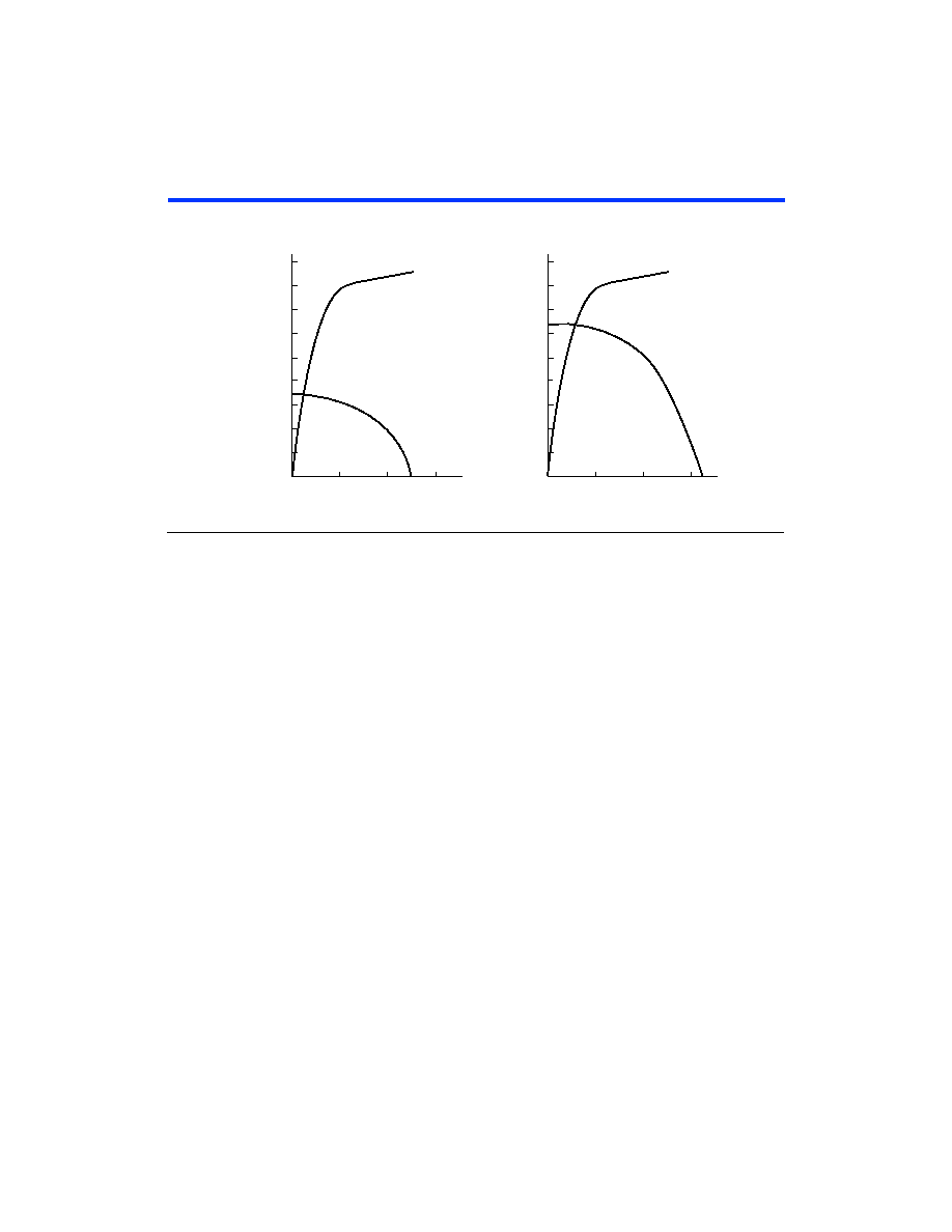
Figure 23. Output Drive Characteristics of ACEX 1K Devices
Timing Model
The continuous, high-performance FastTrack Interconnect routing
resources ensure accurate simulation and timing analysis as well as
predictable performance. This predictable performance contrasts with
that of FPGAs, which use a segmented connection scheme and, therefore,
have an unpredictable performance.
Device performance can be estimated by following the signal path from a
source, through the interconnect, to the destination. For example, the
registered performance between two LEs on the same row can be
calculated by adding the following parameters:
■
LE register clock-to-output delay (tCO)
■
Interconnect delay (tSAMEROW)
■
LE look-up table delay (tLUT)
■
LE register setup time (tSU)
The routing delay depends on the placement of the source and destination
LEs. A more complex registered path may involve multiple combinatorial
LEs between the source and destination LEs.
Timing simulation and delay prediction are available with the simulator
and Timing Analyzer, or with industry-standard EDA tools. The
Simulator offers both pre-synthesis functional simulation to evaluate logic
design accuracy and post-synthesis timing simulation with 0.1-ns
resolution. The Timing Analyzer provides point-to-point timing delay
information, setup and hold time analysis, and device-wide performance
analysis.
VO Output Voltage (V)
IOL
IOH
V
VCCINT = 2.5
VCCIO = 2.5
Room Temperature
V
VCCINT = 2.5
VCCIO = 3.3
Room Temperature
12
3
10
20
30
50
60
40
70
80
90
VO Output Voltage (V)
12
3
10
20
30
50
60
40
70
80
90
IOL
O
Typical I
Output
Current (mA)
O
Typical I
Output
Current (mA)
相關PDF資料 |
PDF描述 |
|---|---|
| EP1K50QC208-1 | IC ACEX 1K FPGA 50K 208-PQFP |
| ADM1032ARMZ-2 | IC TEMP MONITOR 85DEG 8MSOP |
| AMM18DRMN-S288 | CONN EDGECARD 36POS .156 EXTEND |
| RSO-2405D/H3 | CONV DC/DC 1W 18-36VIN +/-05VOUT |
| EP1K100FC484-2 | IC ACEX 1K FPGA 100K 484-FBGA |
相關代理商/技術參數 |
參數描述 |
|---|---|
| EP1K100FC484-3 | 功能描述:FPGA - 現場可編程門陣列 FPGA - ACEX 1K 624 LABs 333 IOs RoHS:否 制造商:Altera Corporation 系列:Cyclone V E 柵極數量: 邏輯塊數量:943 內嵌式塊RAM - EBR:1956 kbit 輸入/輸出端數量:128 最大工作頻率:800 MHz 工作電源電壓:1.1 V 最大工作溫度:+ 70 C 安裝風格:SMD/SMT 封裝 / 箱體:FBGA-256 |
| EP1K100FC484-3N | 功能描述:FPGA - 現場可編程門陣列 FPGA - ACEX 1K 624 LABs 333 IOs RoHS:否 制造商:Altera Corporation 系列:Cyclone V E 柵極數量: 邏輯塊數量:943 內嵌式塊RAM - EBR:1956 kbit 輸入/輸出端數量:128 最大工作頻率:800 MHz 工作電源電壓:1.1 V 最大工作溫度:+ 70 C 安裝風格:SMD/SMT 封裝 / 箱體:FBGA-256 |
| EP1K100FI2562 | 制造商:Altera Corporation 功能描述: |
| EP1K100FI256-2 | 功能描述:FPGA - 現場可編程門陣列 FPGA - ACEX 1K 624 LABs 186 IOs RoHS:否 制造商:Altera Corporation 系列:Cyclone V E 柵極數量: 邏輯塊數量:943 內嵌式塊RAM - EBR:1956 kbit 輸入/輸出端數量:128 最大工作頻率:800 MHz 工作電源電壓:1.1 V 最大工作溫度:+ 70 C 安裝風格:SMD/SMT 封裝 / 箱體:FBGA-256 |
| EP1K100FI256-2N | 功能描述:FPGA - 現場可編程門陣列 FPGA - ACEX 1K 624 LABs 186 IOs RoHS:否 制造商:Altera Corporation 系列:Cyclone V E 柵極數量: 邏輯塊數量:943 內嵌式塊RAM - EBR:1956 kbit 輸入/輸出端數量:128 最大工作頻率:800 MHz 工作電源電壓:1.1 V 最大工作溫度:+ 70 C 安裝風格:SMD/SMT 封裝 / 箱體:FBGA-256 |
發布緊急采購,3分鐘左右您將得到回復。