- 您現在的位置:買賣IC網 > PDF目錄22012 > EP1K100FC484-3N (Altera)IC ACEX 1K FPGA 100K 484-FBGA PDF資料下載
參數資料
| 型號: | EP1K100FC484-3N |
| 廠商: | Altera |
| 文件頁數: | 11/86頁 |
| 文件大小: | 0K |
| 描述: | IC ACEX 1K FPGA 100K 484-FBGA |
| 產品培訓模塊: | Three Reasons to Use FPGA's in Industrial Designs |
| 標準包裝: | 60 |
| 系列: | ACEX-1K® |
| LAB/CLB數: | 624 |
| 邏輯元件/單元數: | 4992 |
| RAM 位總計: | 49152 |
| 輸入/輸出數: | 333 |
| 門數: | 257000 |
| 電源電壓: | 2.375 V ~ 2.625 V |
| 安裝類型: | 表面貼裝 |
| 工作溫度: | 0°C ~ 85°C |
| 封裝/外殼: | 484-BGA |
| 供應商設備封裝: | 484-FBGA(23x23) |
| 其它名稱: | 544-2368 EP1K100FC484-3N-ND |
第1頁第2頁第3頁第4頁第5頁第6頁第7頁第8頁第9頁第10頁當前第11頁第12頁第13頁第14頁第15頁第16頁第17頁第18頁第19頁第20頁第21頁第22頁第23頁第24頁第25頁第26頁第27頁第28頁第29頁第30頁第31頁第32頁第33頁第34頁第35頁第36頁第37頁第38頁第39頁第40頁第41頁第42頁第43頁第44頁第45頁第46頁第47頁第48頁第49頁第50頁第51頁第52頁第53頁第54頁第55頁第56頁第57頁第58頁第59頁第60頁第61頁第62頁第63頁第64頁第65頁第66頁第67頁第68頁第69頁第70頁第71頁第72頁第73頁第74頁第75頁第76頁第77頁第78頁第79頁第80頁第81頁第82頁第83頁第84頁第85頁第86頁
Altera Corporation
19
ACEX 1K Programmable Logic Device Family Data Sheet
D
e
ve
lo
pm
e
n
t
13
To
o
ls
Cascade Chain
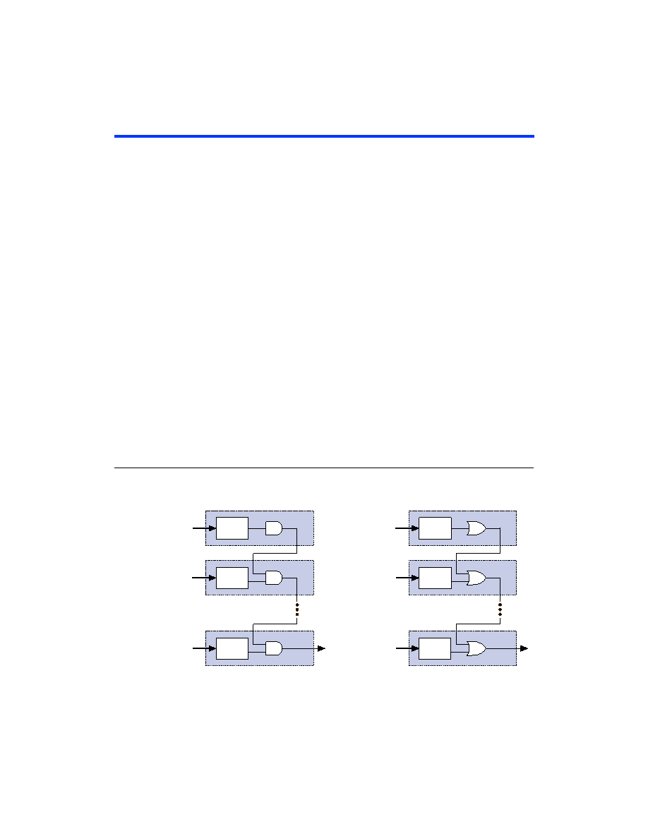
With the cascade chain, the ACEX 1K architecture can implement
functions that have a very wide fan-in. Adjacent LUTs can be used to
compute portions of the function in parallel; the cascade chain serially
connects the intermediate values. The cascade chain can use a logical AND
or logical OR (via De Morgan’s inversion) to connect the outputs of
adjacent LEs. With a delay as low as 0.6 ns per LE, each additional LE
provides four more inputs to the effective width of a function. Cascade
chain logic can be created automatically by the compiler during design
processing, or manually by the designer during design entry.
Cascade chains longer than eight bits are implemented automatically by
linking several LABs together. For easier routing, a long cascade chain
skips every other LAB in a row. A cascade chain longer than one LAB
skips either from even-numbered LAB to even-numbered LAB, or from
odd-numbered LAB to odd-numbered LAB (e.g., the last LE of the first
LAB in a row cascades to the first LE of the third LAB). The cascade chain
does not cross the center of the row (e.g., in the EP1K50 device, the cascade
chain stops at the eighteenth LAB, and a new one begins at the nineteenth
LAB). This break is due to the EAB’s placement in the middle of the row.
Figure 10 shows how the cascade function can connect adjacent LEs to
form functions with a wide fan-in. These examples show functions of 4n
variables implemented with n LEs. The LE delay is 1.3 ns; the cascade
chain delay is 0.6 ns. With the cascade chain, decoding a 16-bit address
requires 3.1 ns.
Figure 10. ACEX 1K Cascade Chain Operation
LE1
LUT
LE2
LUT
d[3..0]
d[7..4]
d[(4
n – 1)..(4n – 4)]
d[3..0]
d[7..4]
LE
n
LE1
LE2
LE
n
LUT
AND Cascade Chain
OR Cascade Chain
d[(4
n – 1)..(4n – 4)]
相關PDF資料 |
PDF描述 |
|---|---|
| TAP686M010BRW | CAP TANT 68UF 10V 20% RADIAL |
| EPF10K30ETC144-3 | IC FLEX 10KE FPGA 30K 144-TQFP |
| VI-BNH-CX | CONVERTER MOD DC/DC 52V 75W |
| RS1K | DIODE GPP FAST 1A 800V SMA |
| VI-BNH-CW | CONVERTER MOD DC/DC 52V 100W |
相關代理商/技術參數 |
參數描述 |
|---|---|
| EP1K100FI2562 | 制造商:Altera Corporation 功能描述: |
| EP1K100FI256-2 | 功能描述:FPGA - 現場可編程門陣列 FPGA - ACEX 1K 624 LABs 186 IOs RoHS:否 制造商:Altera Corporation 系列:Cyclone V E 柵極數量: 邏輯塊數量:943 內嵌式塊RAM - EBR:1956 kbit 輸入/輸出端數量:128 最大工作頻率:800 MHz 工作電源電壓:1.1 V 最大工作溫度:+ 70 C 安裝風格:SMD/SMT 封裝 / 箱體:FBGA-256 |
| EP1K100FI256-2N | 功能描述:FPGA - 現場可編程門陣列 FPGA - ACEX 1K 624 LABs 186 IOs RoHS:否 制造商:Altera Corporation 系列:Cyclone V E 柵極數量: 邏輯塊數量:943 內嵌式塊RAM - EBR:1956 kbit 輸入/輸出端數量:128 最大工作頻率:800 MHz 工作電源電壓:1.1 V 最大工作溫度:+ 70 C 安裝風格:SMD/SMT 封裝 / 箱體:FBGA-256 |
| EP1K100FI484-2 | 功能描述:FPGA - 現場可編程門陣列 FPGA - ACEX 1K 624 LABs 333 IOs RoHS:否 制造商:Altera Corporation 系列:Cyclone V E 柵極數量: 邏輯塊數量:943 內嵌式塊RAM - EBR:1956 kbit 輸入/輸出端數量:128 最大工作頻率:800 MHz 工作電源電壓:1.1 V 最大工作溫度:+ 70 C 安裝風格:SMD/SMT 封裝 / 箱體:FBGA-256 |
| EP1K100FI484-2N | 功能描述:FPGA - 現場可編程門陣列 FPGA - ACEX 1K 624 LABs 333 IOs RoHS:否 制造商:Altera Corporation 系列:Cyclone V E 柵極數量: 邏輯塊數量:943 內嵌式塊RAM - EBR:1956 kbit 輸入/輸出端數量:128 最大工作頻率:800 MHz 工作電源電壓:1.1 V 最大工作溫度:+ 70 C 安裝風格:SMD/SMT 封裝 / 箱體:FBGA-256 |
發布緊急采購,3分鐘左右您將得到回復。