- 您現(xiàn)在的位置:買賣IC網(wǎng) > PDF目錄22010 > EP1K100FI256-2N (Altera)IC ACEX 1K FPGA 100K 256-FBGA PDF資料下載
參數(shù)資料
| 型號: | EP1K100FI256-2N |
| 廠商: | Altera |
| 文件頁數(shù): | 4/86頁 |
| 文件大小: | 0K |
| 描述: | IC ACEX 1K FPGA 100K 256-FBGA |
| 產(chǎn)品培訓模塊: | Three Reasons to Use FPGA's in Industrial Designs |
| 標準包裝: | 90 |
| 系列: | ACEX-1K® |
| LAB/CLB數(shù): | 624 |
| 邏輯元件/單元數(shù): | 4992 |
| RAM 位總計: | 49152 |
| 輸入/輸出數(shù): | 186 |
| 門數(shù): | 257000 |
| 電源電壓: | 2.375 V ~ 2.625 V |
| 安裝類型: | 表面貼裝 |
| 工作溫度: | -40°C ~ 85°C |
| 封裝/外殼: | 256-BGA |
| 供應商設(shè)備封裝: | 256-FBGA(17x17) |
第1頁第2頁第3頁當前第4頁第5頁第6頁第7頁第8頁第9頁第10頁第11頁第12頁第13頁第14頁第15頁第16頁第17頁第18頁第19頁第20頁第21頁第22頁第23頁第24頁第25頁第26頁第27頁第28頁第29頁第30頁第31頁第32頁第33頁第34頁第35頁第36頁第37頁第38頁第39頁第40頁第41頁第42頁第43頁第44頁第45頁第46頁第47頁第48頁第49頁第50頁第51頁第52頁第53頁第54頁第55頁第56頁第57頁第58頁第59頁第60頁第61頁第62頁第63頁第64頁第65頁第66頁第67頁第68頁第69頁第70頁第71頁第72頁第73頁第74頁第75頁第76頁第77頁第78頁第79頁第80頁第81頁第82頁第83頁第84頁第85頁第86頁
12
Altera Corporation
ACEX 1K Programmable Logic Device Family Data Sheet
EABs can be used to implement synchronous RAM, which is easier to use
than asynchronous RAM. A circuit using asynchronous RAM must
generate the RAM write enable signal, while ensuring that its data and
address signals meet setup and hold time specifications relative to the
write enable signal. In contrast, the EAB’s synchronous RAM generates its
own write enable signal and is self-timed with respect to the input or write
clock. A circuit using the EAB’s self-timed RAM must only meet the setup
and hold time specifications of the global clock.
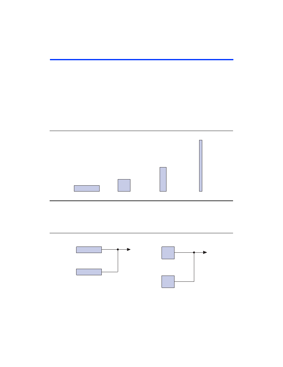
When used as RAM, each EAB can be configured in any of the following
sizes: 256
× 16; 512 × 8; 1,024 × 4; or 2,048 × 2. Figure 5 shows the ACEX 1K
EAB memory configurations.
Figure 5. ACEX 1K EAB Memory Configurations
Larger blocks of RAM are created by combining multiple EABs. For
example, two 256
× 16 RAM blocks can be combined to form a 256 × 32
block, and two 512
× 8 RAM blocks can be combined to form a
512
× 16 block. Figure 6 shows examples of multiple EAB combination.
Figure 6. Examples of Combining ACEX 1K EABs
256
× 16
512
× 8
1,024
× 4
2,048
× 2
512
× 8
512
× 8
256
× 16
256
× 16
256
× 32
512
× 16
相關(guān)PDF資料 |
PDF描述 |
|---|---|
| EP1K100FI256-2 | IC ACEX 1K FPGA 100K 256-FBGA |
| A42MX16-VQG100 | IC FPGA 140I/O 100VQFP |
| A42MX09-TQG176 | IC FPGA 104I/O 176TQFP |
| A42MX16-PQG100 | IC FPGA 140I/O 100PQFP |
| AGL600V5-FGG484 | IC FPGA IGLOO 1.5V 484FPBGA |
相關(guān)代理商/技術(shù)參數(shù) |
參數(shù)描述 |
|---|---|
| EP1K100FI484-2 | 功能描述:FPGA - 現(xiàn)場可編程門陣列 FPGA - ACEX 1K 624 LABs 333 IOs RoHS:否 制造商:Altera Corporation 系列:Cyclone V E 柵極數(shù)量: 邏輯塊數(shù)量:943 內(nèi)嵌式塊RAM - EBR:1956 kbit 輸入/輸出端數(shù)量:128 最大工作頻率:800 MHz 工作電源電壓:1.1 V 最大工作溫度:+ 70 C 安裝風格:SMD/SMT 封裝 / 箱體:FBGA-256 |
| EP1K100FI484-2N | 功能描述:FPGA - 現(xiàn)場可編程門陣列 FPGA - ACEX 1K 624 LABs 333 IOs RoHS:否 制造商:Altera Corporation 系列:Cyclone V E 柵極數(shù)量: 邏輯塊數(shù)量:943 內(nèi)嵌式塊RAM - EBR:1956 kbit 輸入/輸出端數(shù)量:128 最大工作頻率:800 MHz 工作電源電壓:1.1 V 最大工作溫度:+ 70 C 安裝風格:SMD/SMT 封裝 / 箱體:FBGA-256 |
| EP1K100QC208-1 | 功能描述:FPGA - 現(xiàn)場可編程門陣列 FPGA - ACEX 1K 624 LABs 147 IOs RoHS:否 制造商:Altera Corporation 系列:Cyclone V E 柵極數(shù)量: 邏輯塊數(shù)量:943 內(nèi)嵌式塊RAM - EBR:1956 kbit 輸入/輸出端數(shù)量:128 最大工作頻率:800 MHz 工作電源電壓:1.1 V 最大工作溫度:+ 70 C 安裝風格:SMD/SMT 封裝 / 箱體:FBGA-256 |
| EP1K100QC208-1N | 功能描述:FPGA - 現(xiàn)場可編程門陣列 FPGA - ACEX 1K 624 LABs 147 IOs RoHS:否 制造商:Altera Corporation 系列:Cyclone V E 柵極數(shù)量: 邏輯塊數(shù)量:943 內(nèi)嵌式塊RAM - EBR:1956 kbit 輸入/輸出端數(shù)量:128 最大工作頻率:800 MHz 工作電源電壓:1.1 V 最大工作溫度:+ 70 C 安裝風格:SMD/SMT 封裝 / 箱體:FBGA-256 |
| EP1K100QC208-2 | 功能描述:FPGA - 現(xiàn)場可編程門陣列 FPGA - ACEX 1K 624 LABs 147 IOs RoHS:否 制造商:Altera Corporation 系列:Cyclone V E 柵極數(shù)量: 邏輯塊數(shù)量:943 內(nèi)嵌式塊RAM - EBR:1956 kbit 輸入/輸出端數(shù)量:128 最大工作頻率:800 MHz 工作電源電壓:1.1 V 最大工作溫度:+ 70 C 安裝風格:SMD/SMT 封裝 / 箱體:FBGA-256 |
發(fā)布緊急采購,3分鐘左右您將得到回復。