- 您現在的位置:買賣IC網 > PDF目錄16549 > EVAL-ADF4351EB1Z (Analog Devices Inc)BOARD 1 EVAL FOR ADF4351 PDF資料下載
參數資料
| 型號: | EVAL-ADF4351EB1Z |
| 廠商: | Analog Devices Inc |
| 文件頁數: | 1/28頁 |
| 文件大小: | 0K |
| 描述: | BOARD 1 EVAL FOR ADF4351 |
| 標準包裝: | 1 |
| 系列: | * |
當前第1頁第2頁第3頁第4頁第5頁第6頁第7頁第8頁第9頁第10頁第11頁第12頁第13頁第14頁第15頁第16頁第17頁第18頁第19頁第20頁第21頁第22頁第23頁第24頁第25頁第26頁第27頁第28頁
Wideband Synthesizer
with Integrated VCO
Data Sheet
Rev. 0
Information furnished by Analog Devices is believed to be accurate and reliable. However, no
responsibilityis assumedbyAnalogDevicesforitsuse,norforanyinfringementsof patentsorother
rightsofthirdpartiesthatmayresultfromitsuse.Specificationssubjecttochangewithoutnotice.No
license is granted by implication or otherwise under any patent or patent rights of Analog Devices.
Trademarksandregisteredtrademarksarethepropertyoftheirrespectiveowners.
One Technology Way, P.O. Box 9106, Norwood, MA 02062-9106, U.S.A.
Tel: 781.329.4700
Fax: 781.461.3113
2012 Analog Devices, Inc. All rights reserved.
FEATURES
Output frequency range: 35 MHz to 4400 MHz
Fractional-N synthesizer and integer-N synthesizer
Low phase noise VCO
Programmable divide-by-1/-2/-4/-8/-16/-32/-64 output
Typical jitter: 0.3 ps rms
Typical EVM at 2.1 GHz: 0.4%
Power supply: 3.0 V to 3.6 V
Logic compatibility: 1.8 V
Programmable dual-modulus prescaler of 4/5 or 8/9
Programmable output power level
RF output mute function
3-wire serial interface
Analog and digital lock detect
Switched bandwidth fast lock mode
Cycle slip reduction
APPLICATIONS
Wireless infrastructure (W-CDMA, TD-SCDMA, WiMAX,
GSM, PCS, DCS, DECT)
Test equipment
Wireless LANs, CATV equipment
Clock generation
GENERAL DESCRIPTION
The ADF4351 allows implementation of fractional-N or integer-N
phase-locked loop (PLL) frequency synthesizers when used with
an external loop filter and external reference frequency.
The ADF4351 has an integrated voltage controlled oscillator (VCO)
with a fundamental output frequency ranging from 2200 MHz to
4400 MHz. In addition, divide-by-1/-2/-4/-8/-16/-32/-64 circuits
allow the user to generate RF output frequencies as low as 35 MHz.
For applications that require isolation, the RF output stage can be
muted. The mute function is both pin- and software-controllable.
An auxiliary RF output is also available, which can be powered
down when not in use.
Control of all on-chip registers is through a simple 3-wire interface.
The device operates with a power supply ranging from 3.0 V to
3.6 V and can be powered down when not in use.
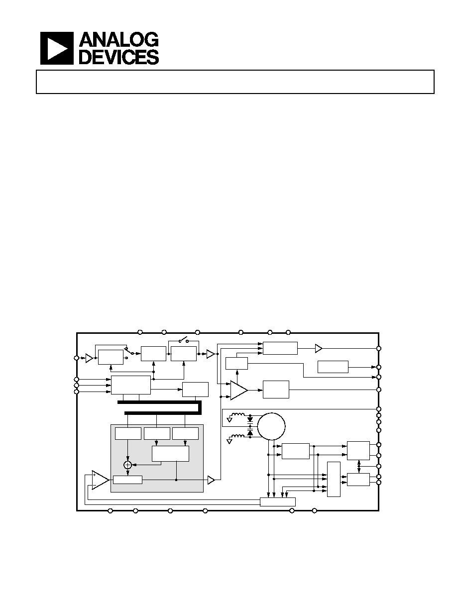
FUNCTIONAL BLOCK DIAGRAM
MUXOUT
CPOUT
LD
SW
VCOM
TEMP
REFIN
CLK
DATA
LE
AVDD
SDVDD
DVDD
VP
AGND
CE
DGND
CPGND
SDGND
AGNDVCO
RSET
VVCO
VTUNE
VREF
RFOUTA+
RFOUTA–
RFOUTB+
RFOUTB–
PHASE
COMPARATOR
FAST LOCK
SWITCH
CHARGE
PUMP
OUTPUT
STAGE
OUTPUT
STAGE
PDBRF
MULTIPLEXER
M
U
LTIP
LE
X
E
R
10-BIT R
COUNTER
÷2
DIVIDER
×2
DOUBLER
FUNCTION
LATCH
DATA REGISTER
INTEGER
VALUE
N COUNTER
FRACTION
VALUE
THIRD-ORDER
FRACTIONAL
INTERPOLATOR
MODULUS
VALUE
MULTIPLEXER
LOCK
DETECT
÷1/2/4/8/16/
32/64
ADF4351
VCO
CORE
09800-
0
01
Figure 1.
相關PDF資料 |
PDF描述 |
|---|---|
| GEM25DRYF | CONN EDGECARD 50POS DIP .156 SLD |
| GEM28DRTF | CONN EDGECARD 56POS DIP .156 SLD |
| H3AWH-4006G | IDC CABLE - HSC40H/AE40G/HPL40H |
| GEM28DRKF | CONN EDGECARD 56POS DIP .156 SLD |
| M1CXA-5036J | IDC CABLE - MKC50A/MC50G/X |
相關代理商/技術參數 |
參數描述 |
|---|---|
| EVAL-ADF4360-0EB1 | 制造商:AD 制造商全稱:Analog Devices 功能描述:Integrated Synthesizer and VCO |
| EVAL-ADF4360-1EB1 | 制造商:Analog Devices 功能描述:Evaluation Board For ADF4360-1 |
| EVAL-ADF4360-1EBZ1 | 功能描述:BOARD EVALUATION FOR ADF4360-1 RoHS:是 類別:編程器,開發系統 >> 評估演示板和套件 系列:- 產品培訓模塊:Obsolescence Mitigation Program 標準包裝:1 系列:- 主要目的:電源管理,電池充電器 嵌入式:否 已用 IC / 零件:MAX8903A 主要屬性:1 芯鋰離子電池 次要屬性:狀態 LED 已供物品:板 |
| EVAL-ADF4360-2EB1 | 制造商:Analog Devices 功能描述:EVALUATION BOARD FOR ADF4360-2 |
| EVAL-ADF4360-2EBZ1 | 功能描述:BOARD EVALUATION FOR ADF4360-2 RoHS:是 類別:編程器,開發系統 >> 評估演示板和套件 系列:- 標準包裝:1 系列:PSoC® 主要目的:電源管理,熱管理 嵌入式:- 已用 IC / 零件:- 主要屬性:- 次要屬性:- 已供物品:板,CD,電源 |
發布緊急采購,3分鐘左右您將得到回復。