- 您現在的位置:買賣IC網 > PDF目錄59889 > F339F-FREQ-HF1000 (FOX ELECTRONICS) CRYSTAL OSCILLATOR, CLOCK, 4 MHz - 54 MHz, HCMOS OUTPUT PDF資料下載
參數資料
| 型號: | F339F-FREQ-HF1000 |
| 廠商: | FOX ELECTRONICS |
| 元件分類: | XO, clock |
| 英文描述: | CRYSTAL OSCILLATOR, CLOCK, 4 MHz - 54 MHz, HCMOS OUTPUT |
| 封裝: | ROHS COMPLIANT, SMD, 6 PIN |
| 文件頁數: | 1/2頁 |
| 文件大小: | 175K |
| 代理商: | F339F-FREQ-HF1000 |
FOXElectronics 5570 Enterprise Parkway Fort Myers, Florida 33905 USA +1.239.693.0099 FAX +1.239.693.1554 http://www.foxonline.com
EMEA Tel/Fax: +44 .1767.312632 | Asia Hong Kong Tel: +852.2854.4285 Fax +852.2854.4282
| Japan Tel: +81.3.3374/2079 Fax: +81.3.3374.5221
2009 FOX ELECTRONICS | ISO9001:2000 Certified
HCMOS 3.2x2.5mm 3.3V SMD Oscillator
Rev. 7/8/2009
RoHS Compliant / Pb Free
Model: F337/F339 Series
Page 1 of 2
OUTPUT (Pin 3)
ACTIVE
High Z
EnAblE / DiSAblE FunCtiOn
INH (Pin 1)
OPEN 2
'1' Level Vih
≥ 70% Vdd
'0' Level Vil
≤ 30% Vdd
FEAtuRES
3.3V Operation
HCMOS Output
Standby Function
Tape and Reel (1,000 pcs. STD)
Frequency
Stability1
±15PPM
±10PPM
Operating
Temperature (C)
-20 ~ +70
-40 ~ +85
-20 ~ +70
-40 ~ +85
Frequency
Range (MHz)
4.000 ~ 54.000
F337F
F337R
F339F
F339R
Model
Number
Part Number
826B-Frequency-xxxxx
826C-Frequency-xxxxx
826-Frequency-xxxxx
826A-Frequency-xxxxx
PARt nuMbER SElECtiOn Learn More - Internet Required
4.000 ~ 54.000 MHz
-40C ~ +85C
3.3V ± 5%
7mA
45% ~ 55%
5nS
10% Vdd
90% Vdd Min
4mA Min
-4mA Min
15pF
10A
10mS
250nS
10mS
-145dBc/Hz Typ.
3pS RMS Typ.
260C / 10 Seconds
1
Au
PARAMETERS
Frequency Range
(Fo)
Storage Temperature Range (Tstg)
Supply Voltage
(Vdd)
Input Current
(Idd)
Output Symmetry (50% Vdd)
Rise Time (10% ~ 90% Vdd)
Fall Time (90% ~ 10% Vdd)
Output Voltage
(Vol)
(Voh)
Output Current
(Iol)
(Ioh)
Output Load
(HCMOS)
Standby Current
(Istd)
Start-up Time
(Ts)
Output Disable Time 2
Output Enable Time 2
Phase Noise
(@ 10kHz offset)
Period Jitter
Reflow Soldering Temp / Time
Moisture Sensitivity Level (MSL)
Termination Finish
ElECtRiCAl CHARACtERiStiCS
MAX (unless otherwise noted)
1 Inclusive of 25
C tolerance, operating temperature range, input voltage change, load change,
reflow and one year aging.
2
An internal pullup resistor from pin 1 to pin 4 allows active output if pin 1 is left open.
Note: A 0.01F bypass capacitor should be placed between Vdd (Pin 4) and GND (Pin 2) to
minimize power supply line noise.
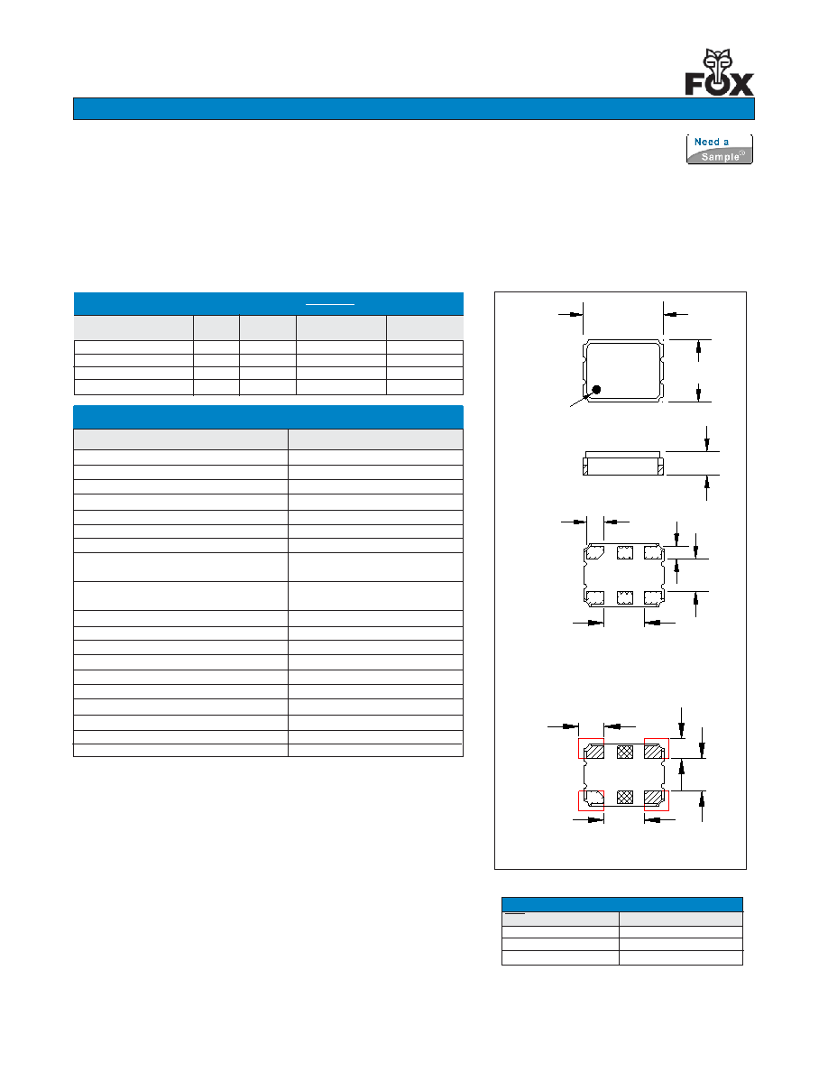
Drawing is for reference to critical specifications defined by size measurements.
Certain non-critical visual attributes, such as side castellations, reference pin shape, etc. may
vary. All specifications subject to change without notice.
Pin Connection
#1 E/D**
#3 Output
#2 GND
#4 Vdd
3.3 Max
1.0 Max
Solder Pad Layout
Recommended
2.6 Max
0.7
0.5
1.3
#1
#4
#3
#2
Top
View
Bottom
View
Dot denotes
Pin 1
All dimensions are in millimeters.
1.6
#1
TP
#2
#4
TP
#3
#1
TP = Test Point and is No Connect
1.0
1.6
0.8
1.3
MARKING
相關PDF資料 |
PDF描述 |
|---|---|
| F337R-FREQ-FM1000 | CRYSTAL OSCILLATOR, CLOCK, 4 MHz - 54 MHz, HCMOS OUTPUT |
| F337F-FREQ-FF0 | CRYSTAL OSCILLATOR, CLOCK, 4 MHz - 54 MHz, HCMOS OUTPUT |
| F337MPL | 1 FUNCTIONS, 31.5 MHz, SAW-VIDEO/SOUND FILTER |
| F3400R1.544MHZBM0 | CRYSTAL OSCILLATOR, CLOCK, 1.544 MHz, HCMOS/TTL OUTPUT |
| F3410R50.000MHZAM0 | CRYSTAL OSCILLATOR, CLOCK, 50 MHz, HCMOS/TTL OUTPUT |
相關代理商/技術參數 |
參數描述 |
|---|---|
| F339MX221031JC02G0 | 制造商:Vishay BCcomponents 功能描述:MKP 0.001?F ?5% 310VACX2 (M) E3 - Ammo Pack |
| F339MX221031JCA2B0 | 制造商:Vishay BCcomponents 功能描述:MKP 0.001?F ?5% 310VACX2 (M) E3 - Bulk |
| F339MX221031JCI2B0 | 制造商:Vishay BCcomponents 功能描述:MKP 0.001?F ?5% 310VACX2 (M) E3 - Bulk |
| F339MX221031JCM2B0 | 制造商:Vishay BCcomponents 功能描述:MKP 0.001?F ?5% 310VACX2 (M) E3 - Bulk |
| F339MX221031JD02G0 | 制造商:Vishay BCcomponents 功能描述:MKP 0.001?F ?5% 310VACX2 (M) E120 - Ammo Pack |
發布緊急采購,3分鐘左右您將得到回復。