- 您現在的位置:買賣IC網 > PDF目錄375723 > FAN4855 (Fairchild Semiconductor Corporation) 500mA High Efficiency Boost Regulator with Adjustable Output, Shutdown and Low Battery Detect PDF資料下載
參數資料
| 型號: | FAN4855 |
| 廠商: | Fairchild Semiconductor Corporation |
| 英文描述: | 500mA High Efficiency Boost Regulator with Adjustable Output, Shutdown and Low Battery Detect |
| 中文描述: | 500mA的高效率升壓可調輸出,關機和低電池檢測穩壓器 |
| 文件頁數: | 8/13頁 |
| 文件大小: | 148K |
| 代理商: | FAN4855 |
PRODUCT SPECIFICATION
FAN4855
8
REV. 1.0.0 3/17/04
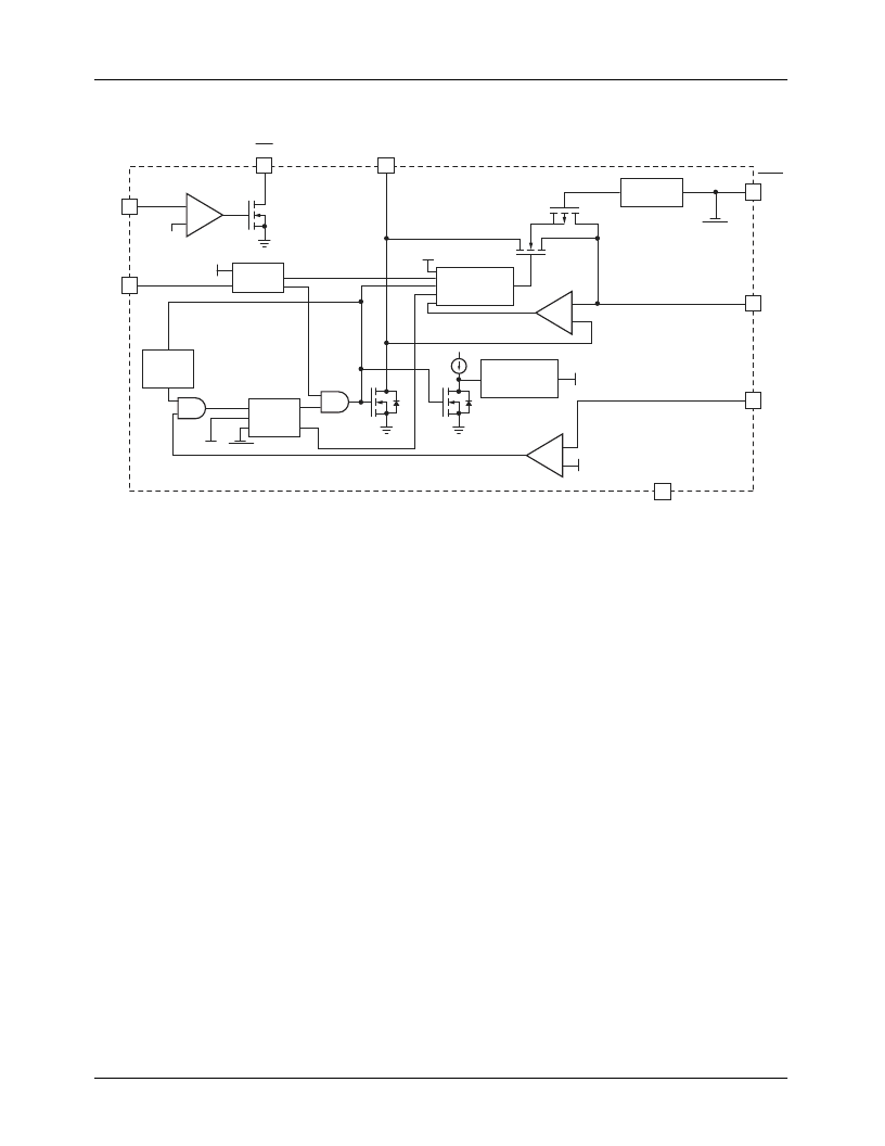
Block Diagram
Functional Description
Boost Regulator
FAN4855 is an adjustable boost regulator that combines
variable ON and minimum OFF architecture with synchro-
nous rectification. Unique control circuitry provides high-
efficiency power conversion for both light and heavy loads
by transitioning between discontinuous and continuous
conduction mode based on load conditions. There is no
oscillator; a constant-peak-current limit of 0.8A in the
inductor allows the inductor current to vary between this
peak limit and some lesser value. The switching frequency
depends upon the load, the input and output voltage ranging
up to 430kHz.
The input voltage V
IN
comes to V
IN
pin and through the
external inductor to the V
L
pin of the device. The loop from
V
OUT
closes through the external resistive voltage divider to
the feedback pin V
FB
. The transfer ratio of this divider deter-
mines the output voltage. When V
FB
voltage drops below the
V
REF
= 1.24V the error amplifier A1 signals to regulator to
deliver charge to the output by triggering the Variable On-
Time One Shot. One Shot generates a pulse at the gate of the
Power NMOS transistor Q1. This transistor will charge the
Inductor L1 for the time interval T
ON
resulting in a peak
current given by:
When the one–shot times out, the Q1 transistor releases the
V
L
pin, allowing the inductor to fly-back and momentarly
charge the output through the body diode of the transistor
Q2. But, as the voltage across the Q2 changes polarity, its
gate will be driven low by the Synchronous Rectifier Control
Circuit (SRC), causing Q2 to short out its body diode. The
inductor then delivers the charge to the load by discharging
into it through Q2.
Under light load conditions, the amount of energy delivered
in this single pulse satisfies the voltage-control loop, and the
converter does not command any more energy pulses until
the output drops again below the lower-voltage threshold.
Under medium and heavy loads, a single energy pulse is not
sufficient to force the output voltage above its upper thresh-
old before the minimum off time has expired and a second
charge cycle is commanded. Since the inductor current has
not reached zero in this case, the peak current is greater than
the previous value at the end of the second cycle. The result
is a ratcheting of inductor current until either the output volt-
age is satisfied, or the converter reaches its set current limit.
After a period of time T
OFF
> 1μS, determined by Minimum
Off–Time Logic and if V
OUT
is low (V
FB
< V
REF
), the
Variable On-Time One Shot will be turned ON again and
the process repeats.
The output capacitor of the converter filters the variable
component, limiting the output voltage ripple to a value
determined by its capacitance and its ESR.
LBO
SHDN
Start-Up
Minimum
Off-Time
Logic
Variable
On-Time
One Shot
Current
Limit
Control
Synchronous
Rectifier
Control
4
7
2
6
5
8
3
1
V
IN
V
L
V
OUT
I
LIMIT
I
LIMIT
V
REF
V
OUT
GND
V
FB
I
LIMIT
SHDN
N
1
LBI
Q
1
Q
2
0.39V
A3
Control
Logic
A2
A1
–
+
–
+
–
+
SHDN
I
L PEAK
)
T
--------------------------
V
×
L
1
=
相關PDF資料 |
PDF描述 |
|---|---|
| FAN4855MTC | 500mA High Efficiency Boost Regulator with Adjustable Output, Shutdown and Low Battery Detect |
| FAN4855MTCX | 500mA High Efficiency Boost Regulator with Adjustable Output, Shutdown and Low Battery Detect |
| FAN4855MU | 500mA High Efficiency Boost Regulator with Adjustable Output, Shutdown and Low Battery Detect |
| FAN4855MUX | 500mA High Efficiency Boost Regulator with Adjustable Output, Shutdown and Low Battery Detect |
| FAN5009 | Dual Bootstrapped 12V MOSFET Driver |
相關代理商/技術參數 |
參數描述 |
|---|---|
| FAN4855MTC | 功能描述:直流/直流開關調節器 Adj 2-Cell Boost RoHS:否 制造商:International Rectifier 最大輸入電壓:21 V 開關頻率:1.5 MHz 輸出電壓:0.5 V to 0.86 V 輸出電流:4 A 輸出端數量: 最大工作溫度: 安裝風格:SMD/SMT 封裝 / 箱體:PQFN 4 x 5 |
| FAN4855MTCX | 功能描述:直流/直流開關調節器 Adj 2-Cell Boost RoHS:否 制造商:International Rectifier 最大輸入電壓:21 V 開關頻率:1.5 MHz 輸出電壓:0.5 V to 0.86 V 輸出電流:4 A 輸出端數量: 最大工作溫度: 安裝風格:SMD/SMT 封裝 / 箱體:PQFN 4 x 5 |
| FAN4855MTCX | 制造商:Fairchild Semiconductor Corporation 功能描述:DC/DC Converter IC |
| FAN4855MU | 制造商:FAIRCHILD 制造商全稱:Fairchild Semiconductor 功能描述:500mA High Efficiency Boost Regulator with Adjustable Output, Shutdown and Low Battery Detect |
| FAN4855MUX | 制造商:FAIRCHILD 制造商全稱:Fairchild Semiconductor 功能描述:500mA High Efficiency Boost Regulator with Adjustable Output, Shutdown and Low Battery Detect |
發布緊急采購,3分鐘左右您將得到回復。