- 您現在的位置:買賣IC網 > PDF目錄375723 > FAN5063M (FAIRCHILD SEMICONDUCTOR CORP) Power Supply Switching Circuit PDF資料下載
參數資料
| 型號: | FAN5063M |
| 廠商: | FAIRCHILD SEMICONDUCTOR CORP |
| 元件分類: | 模擬信號調理 |
| 英文描述: | Power Supply Switching Circuit |
| 中文描述: | SPECIALTY ANALOG CIRCUIT, PDSO16 |
| 封裝: | SOIC-16 |
| 文件頁數: | 2/14頁 |
| 文件大小: | 196K |
| 代理商: | FAN5063M |
FAN5063
PRODUCT SPECIFICATION
2
REV. 1.0.0 12/4/00
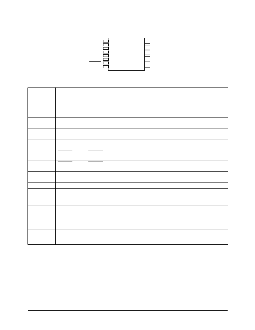
Pin Assignments
Pin Definitions
Pin Number
1
Pin Name
QCAP
Pin Function Description
Charge pump cap.
generate high voltage from standby power.
Charge pump switcher.
5V Standby.
Apply +5V standby on this pin to run the circuit in standby mode.
3.3V main gate control.
Attach this pin to a transistor powering 3.3V dual from
the 3.3V main supply.
3.3V standby gate control.
Attach this pin to a transistor powering 3.3V dual
from the 5V standby supply.
3.3V voltage Feedback.
Pin 6 is used as the input for the voltage feedback
control loop for 3.3V dual.
SLP_S3.
Control signal governing the Soft Off state S3. Internal current source
pulls this line high if left open.
SLP_S5.
Control signal governing the Soft Off state S5. Internal current source
pulls this line high if left open.
PWR_OK.
Control signal for switches. Internal current source pulls this line high if
left open.
Softstart.
Attach a capacitor to this pin to determine the softstart rate.
Ground.
Connect this pin to ground.
Adjustable Dual Voltage Feedback.
Pin 12 is used as the input for the voltage
feedback loop for the adjustable dual voltage.
Adjustable Dual Voltage
. Pin 13 sources VADJ during standby.
Adjustable Dual Voltage Base Control.
Attach this pin to an NPN transistor
powering VADJ from the 5V Main.
5V Main.
Apply +5V Main on this pin to run the VADJ base drive.
Main Power.
Apply +12V through a diode on this pin to run the circuit in normal
mode. Bypass with a 0.1μF capacitor. When 12V is not present, this pin produces
voltage doubled 5V standby.
Attach flying capacitor between this pin and PUMP to
2
3
4
PUMP
5VSTBY
3VOUT1
5
3VOUT2
6
3VFB
7
SLP_S3
8
SLP_S5
9
PWR_OK
10
11
12
SS
GND
VADJFB
13
14
VADJ
VADJOUT
15
16
5VMAIN
VCCP
1
2
3
4
5
6
7
8
16
15
14
13
12
11
10
9
FAN5063
QCAP
PUMP
5VSTBY
3VOUT1
3VOUT2
3VFB
SLP_S3
SLP_S5
VCCP
5VMAIN
VADJOUT
VADJ
VADJFB
GND
SS
PWR_OK
相關PDF資料 |
PDF描述 |
|---|---|
| FAN5066 | Ultra Low Voltage Synchronous DC-DC Controller |
| FAN5066M | |
| FAN5066MTC | |
| FAN5066MTCX | |
| FAN5067 | ACPI Dual Switch Controller |
相關代理商/技術參數 |
參數描述 |
|---|---|
| FAN5063MX | 功能描述:開關變換器、穩壓器與控制器 aCPI Dual Switch Controller RoHS:否 制造商:Texas Instruments 輸出電壓:1.2 V to 10 V 輸出電流:300 mA 輸出功率: 輸入電壓:3 V to 17 V 開關頻率:1 MHz 工作溫度范圍: 安裝風格:SMD/SMT 封裝 / 箱體:WSON-8 封裝:Reel |
| FAN5063-ZCA3026B WAF | 制造商:Fairchild Semiconductor Corporation 功能描述: |
| FAN5066 | 制造商:FAIRCHILD 制造商全稱:Fairchild Semiconductor 功能描述:Ultra Low Voltage Synchronous DC-DC Controller |
| FAN5066A WAF | 制造商:Fairchild Semiconductor Corporation 功能描述: |
| FAN5066A-3116B WAF | 制造商:Fairchild Semiconductor Corporation 功能描述: |
發布緊急采購,3分鐘左右您將得到回復。