- 您現(xiàn)在的位置:買賣IC網(wǎng) > PDF目錄375725 > FAN53168MTC (FAIRCHILD SEMICONDUCTOR CORP) 6-Bit VID Controlled 2-4 Phase DC-DC Controller PDF資料下載
參數(shù)資料
| 型號: | FAN53168MTC |
| 廠商: | FAIRCHILD SEMICONDUCTOR CORP |
| 元件分類: | 穩(wěn)壓器 |
| 英文描述: | 6-Bit VID Controlled 2-4 Phase DC-DC Controller |
| 中文描述: | SWITCHING CONTROLLER, 4000 kHz SWITCHING FREQ-MAX, PDSO28 |
| 封裝: | TSSOP-28 |
| 文件頁數(shù): | 22/28頁 |
| 文件大小: | 397K |
| 代理商: | FAN53168MTC |
第1頁第2頁第3頁第4頁第5頁第6頁第7頁第8頁第9頁第10頁第11頁第12頁第13頁第14頁第15頁第16頁第17頁第18頁第19頁第20頁第21頁當(dāng)前第22頁第23頁第24頁第25頁第26頁第27頁第28頁
FAN53168
PRODUCT SPECIFICATION
22
REV. 1.0.0 6/9/03
With the multimode feedback structure of the FAN53168,
one needs to set the feedback compensation to make the
converter
’
s output impedance working in parallel with the
output decoupling meet this goal. There are several poles and
zeros created by the output inductor and decoupling capaci-
tors (output
fi
lter) that need to be compensated for.
A type-three compensator on the voltage feedback is
adequate for proper compensation of the output
fi
lter. The
expressions given in Equations 25
–
29 are intended to yield
an optimal starting point for the design; some adjustments
may be necessary to account for PCB and component para-
sitic effects (see the Tuning Procedure for the FAN53168
section).
The
fi
rst step is to compute the time constants for all of the
poles and zeros in the system:
where, for the FAN53168, R’ is the PCB resistance from the
bulk capacitors to the ceramics and where R
DS
is approxi-
mately the total low-side MOSFET ON resistance per phase
at 25oC. For this example, A
D
is 5, V
RT
equals 0.974V, R’ is
approximately 0.6m
(assuming a 4-layer motherboard) and
L
X
is 375pH for the eight Al-Poly capacitors.
The compensation values can then be solved for using the
following:
Choosing the closest standard values for these components
yields: C
A
= 390pF, R
A
= 16.9k
, C
B
= 1.5nF,
and C
FB
= 33pF.
C
IN
Selection and Input Current di/dt Reduction
In continuous inductor-current mode, the source current of
the high-side MOSFET is approximately a square wave with
a duty ratio equal to n (V
OUT
/V
IN
) and an amplitude of one-
nth of the maximum output current. To prevent large voltage
transients, a low ESR input capacitor sized for the maximum
rms current must be used. The maximum rms capacitor
current is given by:
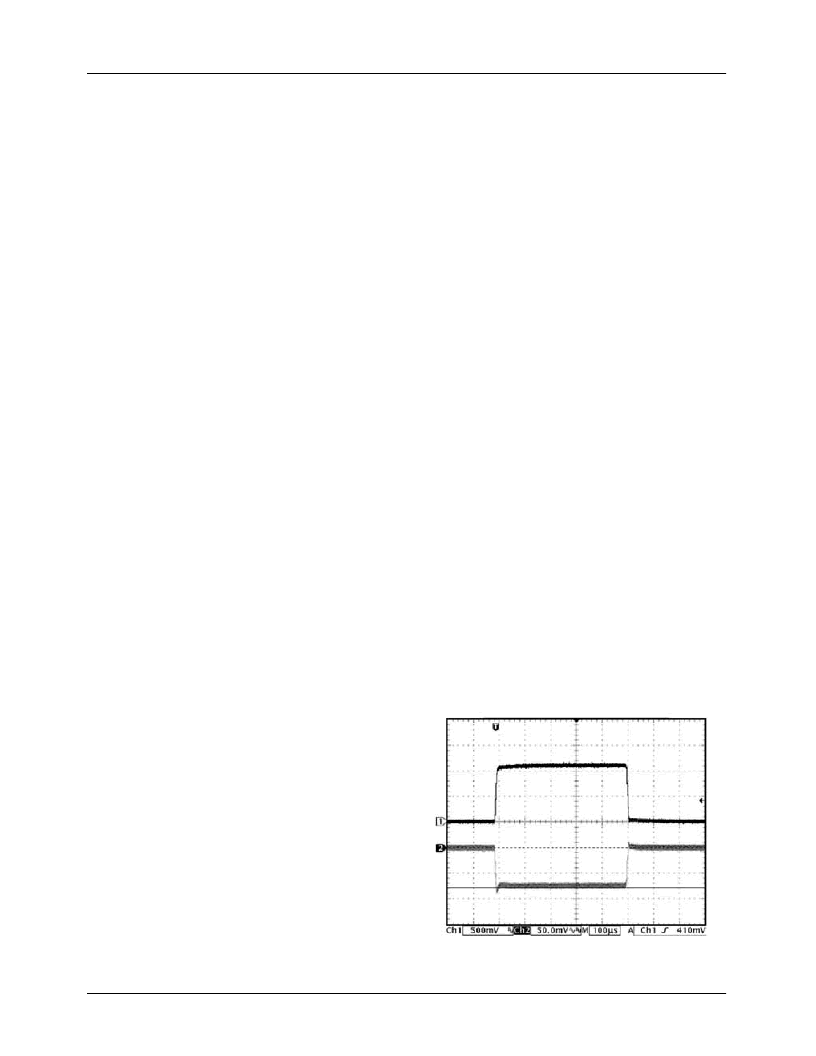
Figure 6. Typical Transient Response for Design Example
R
E
n
R
O
A
D
R
DS
+
R
----------------------
V
×
VID
2
--------------------------------------------------------
L
×
1 n
–
(
X
D
×
)
V
RT
×
×
O
VID
+
+
×
×
=
(25)
R
E
3
1.3m
5
5.95m
-------------------------------------------
+
+
×
+
×
=
----------------------------------------–
)
0.974V
1.5V
×
×
55.3m
=
T
A
C
X
R
O
R
'
–
(
)
L
X
R
O
-------
R
-------------------
R
'
–
X
×
+
×
=
(26)
T
A
6.56mF
1.3
0.6m
–
(
)
------------------
×
+
×
=
--------------------–
4.79
μ
s
=
T
B
R
X
R
'
R
O
–
+
(
)
C
X
×
=
(27)
T
B
1.0m
0.6m
1.3m
–
+
(
)
6.56mF
×
1.97
μ
s
=
=
T
C
V
RT
--------------------------------------------------------
L
A
R
×
------------------------
–
×
VID
E
=
(28)
T
C
0.974V
--------------------------------------------------------------------------------------
650nH
-------------------------------
–
×
6.86
μ
s
=
=
T
D
C
O
C
'
–
C
Z
+
C
X
R
O
------------------------------------------------------------------
=
(29)
T
D
1.3m
220
μ
F
+
(
)
2
×
)
1.3m
×
--------------------------------------------------–
500ns
=
=
C
A
n
------------------------------
R
×
E
T
A
×
B
=
(30)
C
A
----------------------------------------------------
s
253pF
=
=
R
A
T
C
C
A
-------
s
------------------
27.1k
=
=
=
(31)
C
B
T
B
R
B
-------
s
-------------------
1.48nF
=
=
=
(32)
C
FB
T
D
R
A
-------
-------------------
18.5pF
=
=
=
(33)
相關(guān)PDF資料 |
PDF描述 |
|---|---|
| FAN53180MTC | 6-Bit VID Controlled 2-4 Phase DC-DC Controller |
| FAN53180 | 6-Bit VID Controlled 2-4 Phase DC-DC Controller |
| FAN5330 | High Efficiency Serial LED Driver with 30V Integrated Switch |
| FAN5331 | 1.6MHz Boost Converter with 20V Integrated FET Switch |
| FAN5331SX | 1.6MHz Boost Converter with 20V Integrated FET Switch |
相關(guān)代理商/技術(shù)參數(shù) |
參數(shù)描述 |
|---|---|
| FAN53168MTCX | 功能描述:DC/DC 開關(guān)控制器 Buck Controller 2to4 Phs VID Sync RoHS:否 制造商:Texas Instruments 輸入電壓:6 V to 100 V 開關(guān)頻率: 輸出電壓:1.215 V to 80 V 輸出電流:3.5 A 輸出端數(shù)量:1 最大工作溫度:+ 125 C 安裝風(fēng)格: 封裝 / 箱體:CPAK |
| FAN53180 | 制造商:FAIRCHILD 制造商全稱:Fairchild Semiconductor 功能描述:6-Bit VID Controlled 2-4 Phase DC-DC Controller |
| FAN53180MTC | 制造商:FAIRCHILD 制造商全稱:Fairchild Semiconductor 功能描述:6-Bit VID Controlled 2-4 Phase DC-DC Controller |
| FAN53180MTCX | 功能描述:DC/DC 開關(guān)控制器 Buck Controller 2to4 Phs VID Sync RoHS:否 制造商:Texas Instruments 輸入電壓:6 V to 100 V 開關(guān)頻率: 輸出電壓:1.215 V to 80 V 輸出電流:3.5 A 輸出端數(shù)量:1 最大工作溫度:+ 125 C 安裝風(fēng)格: 封裝 / 箱體:CPAK |
| FAN5330 | 制造商:FAIRCHILD 制造商全稱:Fairchild Semiconductor 功能描述:High Efficiency Serial LED Driver with 30V Integrated Switch |
發(fā)布緊急采購,3分鐘左右您將得到回復(fù)。