- 您現(xiàn)在的位置:買賣IC網(wǎng) > Datasheet目錄38 > FAN7930CM (Fairchild Semiconductor)IC PFC CTLR CRITICAL CONF 8-SOIC Datasheet資料下載
參數(shù)資料
| 型號(hào): | FAN7930CM |
| 廠商: | Fairchild Semiconductor |
| 文件頁(yè)數(shù): | 11/22頁(yè) |
| 文件大小: | 1725K |
| 描述: | IC PFC CTLR CRITICAL CONF 8-SOIC |
| 標(biāo)準(zhǔn)包裝: | 95 |
| 模式: | 臨界傳導(dǎo)(CRM) |
| 頻率 - 開(kāi)關(guān): | 250kHz ~ 350kHz |
| 電流 - 啟動(dòng): | 120µA |
| 電源電壓: | 13 V ~ 20 V |
| 工作溫度: | -40°C ~ 125°C |
| 安裝類型: | 表面貼裝 |
| 封裝/外殼: | 8-SOIC(0.154",3.90mm 寬) |
| 供應(yīng)商設(shè)備封裝: | 8-SOP |
| 包裝: | 管件 |
第1頁(yè)第2頁(yè)第3頁(yè)第4頁(yè)第5頁(yè)第6頁(yè)第7頁(yè)第8頁(yè)第9頁(yè)第10頁(yè)當(dāng)前第11頁(yè)第12頁(yè)第13頁(yè)第14頁(yè)第15頁(yè)第16頁(yè)第17頁(yè)第18頁(yè)第19頁(yè)第20頁(yè)第21頁(yè)第22頁(yè)
?2010 Fairchild Semiconductor Corporation
www.fairchildsemi.com
FAN7930C " Rev. 1.0.2
11
Applications Information
1. Startup: Normally, supply voltage (V
CC
) of a PFC
block is fed from the additional power supply, which can
be called standby power. Without this standby power,
auxiliary winding for zero current detection can be used
as a supply source. Once the supply voltage of the PFC
block exceeds 12 V, internal operation is enabled until
the voltage drops to 8.5 V. If V
CC
exceeds V
Z
, 20 mA
current is sinking from V
CC
.
V
CC
V Z
+
-
V
T H ( S / S )
12
8 . 5
V
C C
2 .5 V
R E F
In te r n a l
B ia s
V B I A S
V
R E F
r e s e t
H : o p e n
2 0 m A
P F C In d u c to r
A u x . W in d in g
V
I N
P F C
V
O U T
P F C
E x te r n a l V
C C
c ir c u it
w h e n n o s ta n d b y p o w e r e x is ts
8
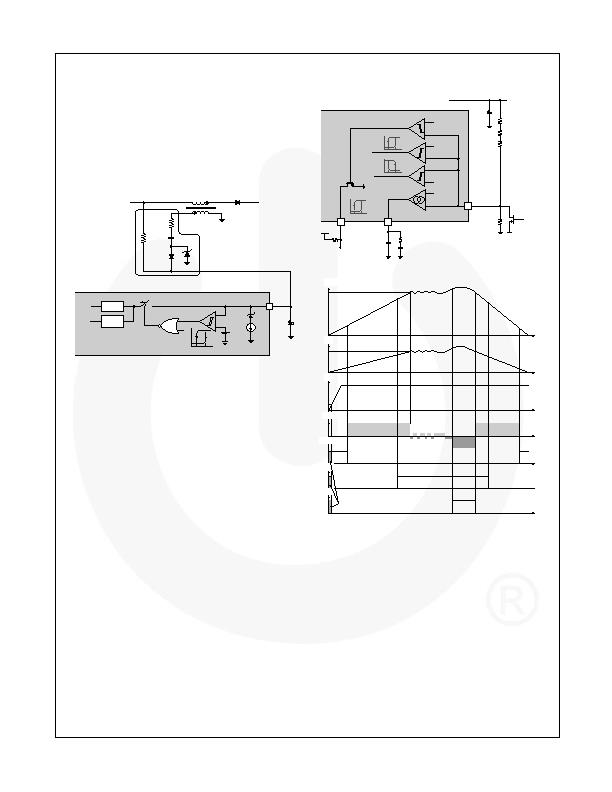
Figure 22. Startup Circuit
2. INV Block: Scaled-down voltage from the output is
the input for the INV pin. Many functions are embedded
based on the INV pin: transconductance amplifier,
output OVP comparator, disable comparator, and output
UVLO comparator.
For the output voltage control, a transconductance
amplifier is used instead of the conventional voltage
amplifier. The transconductance amplifier (voltage-
controlled current source) aids the implementation of
the OVP and disable functions. The output current of
the amplifier changes according to the voltage
difference of the inverting and non-inverting input of
the amplifier. To cancel down the line input voltage
effect on power factor correction, the effective control
response of the PFC block should be slower than the
line frequency and this conflicts with the transient
response of controller. Two-pole one-zero type
compensation can meet both requirements.
The OVP comparator shuts down the output drive block
when the voltage of the INV pin is higher than 2.675 V
and there is 0.175 V hysteresis. The disable comparator
disables operation when the voltage of the inverting input
is lower than 0.35 V and there is 100 mV hysteresis. An
external small-signal MOSFET can be used to disable the
IC, as shown in Figure 23. The IC operating current
decreases to reduce power consumption if the IC is
disabled. Figure 24 is the timing chart of the internal
circuit near the INV pin when rated PFC output voltage
is 390 V
DC
and V
CC
supply voltage is 15 V.
V
O U T
P F C
2. 5 V
0 . 4 5 V / 0 . 3 5 V
I N V o p e n
2 . 6 7 5 V / 2 . 5 V
O V P
2 . 2 4 0 V / 2 . 0 5 1 V
U V L O
2. 2 4 0
2 . 0 5 1
h i g h
CC
d i s a b l e
1
I N V
3
C O M P
2
R D Y
0 . 4 5
0 . 3 5
d i s a b l e
2 . 6 7 5
2 . 5
d i s a b l e
Figure 23. Circuit Around INV Pin
3 9 0 V d c
2 . 5 0 V
2 . 6 5 V
0 . 4 5 V
C u r r e n t s o u r c i n g
C u r r e n t s o u r c i n g
I s i n k i n g
0 . 3 5 V
2 . 0 5 1 V
2 . 2 4 V
2 . 5 0 V
2 . 0 V
3 4 9 V
4 1 3 V
3 9 0 V
3 2 0 V
7 0 V
5 5 V
V
O U T
P F C
V I N V
V C C
I
O U T
C O M P
D i s a b l e
V
R D Y
O V P
V o l t a g e i s d e c i d e d b y p u l l - u p v o l t a g e .
V c c < 2 V , i n t e r n a l l o g i c i s n o t a l i v e .
- R D Y p i n i s f l o a t i n g , s o p u l l u p v o l t a g e i s s h o w n .
- I n t e r n a l s i g n a l s a r e u n k n o w n .
1 5 V
Figure 24. Timing Chart for INV Block
3. RDY Output: When the INV voltage is higher than
2.24 V, RDY output is triggered HIGH and lasts until the
INV voltage is lower than 2.051 V. When input AC
voltage is quite high, for example 240 V
AC
, PFC output
voltage is always higher than RDY threshold, regardless
of boost converter operation. In this case, the INV
voltage is already higher than 2.24 V before PFC V
CC
touches V
START
; however, RDY output is not triggered to
HIGH until V
CC
touches V
START
. After boost converter
operation stops, RDY is not pulled LOW because the
INV voltage is higher than the RDY threshold. When V
CC
of the PFC drops below 5 V, RDY is pulled LOW even
though PFC output voltage is higher than threshold. The
RDY pin output is open drain, so needs an external pull-
up resistor to supply the proper power source. The RDY
pin output remains floating until V
CC
is higher than 2 V.
相關(guān)PDF資料 |
PDF描述 |
|---|---|
| FAN9611MX | IC PFC CTLR DUAL BCM 16-SOIC |
| FAN9612MX | IC CTLR PFC DUAL BCM 16SOICN |
| FL6961MY | IC CTLR PFC SGL FLYBACK 8-SOIC |
| IR1150ISTRPBF | IC PFC CONTROLLER CCM 8-SOIC |
| IR1152STRPBF | IC PFC ONE CYCLE CONTROL 8SOIC |
相關(guān)代理商/技術(shù)參數(shù) |
參數(shù)描述 |
|---|---|
| FAN7930CMX | 功能描述:功率因數(shù)校正 IC Critical Conduction Mode PFC Controller RoHS:否 制造商:Fairchild Semiconductor 開(kāi)關(guān)頻率:300 KHz 最大功率耗散: 最大工作溫度:+ 125 C 安裝風(fēng)格:SMD/SMT 封裝 / 箱體:SOIC-8 封裝:Reel |
| FAN7930CMX_G | 制造商:Fairchild Semiconductor Corporation 功能描述:IC PFC CTLR CRITICAL CONF 8-SOIC 制造商:Fairchild Semiconductor Corporation 功能描述:Power Factor Correction - PFC Critical Conduction Mode PFC Controller 制造商:Fairchild Semiconductor Corporation 功能描述:Critical Conduction Mode PFC Controller |
| FAN7930DM | 制造商:Fairchild Semiconductor Corporation 功能描述:PFC |
| FAN7930DMX | 制造商:Fairchild Semiconductor Corporation 功能描述:PFC |
| FAN7930M | 功能描述:功率因數(shù)校正 IC Critical Conduction Mode PFC Controller RoHS:否 制造商:Fairchild Semiconductor 開(kāi)關(guān)頻率:300 KHz 最大功率耗散: 最大工作溫度:+ 125 C 安裝風(fēng)格:SMD/SMT 封裝 / 箱體:SOIC-8 封裝:Reel |
發(fā)布緊急采購(gòu),3分鐘左右您將得到回復(fù)。