- 您現在的位置:買賣IC網 > PDF目錄375798 > FIN1215MTD (FAIRCHILD SEMICONDUCTOR CORP) LVDS 21-Bit Serializers/De-Serializers PDF資料下載
參數資料
| 型號: | FIN1215MTD |
| 廠商: | FAIRCHILD SEMICONDUCTOR CORP |
| 元件分類: | 通用總線功能 |
| 英文描述: | LVDS 21-Bit Serializers/De-Serializers |
| 中文描述: | TRIPLE LINE DRIVER, PDSO48 |
| 封裝: | 6.10 MM, MO-153, TSSOP-48 |
| 文件頁數: | 7/17頁 |
| 文件大小: | 434K |
| 代理商: | FIN1215MTD |
7
www.fairchildsemi.com
F
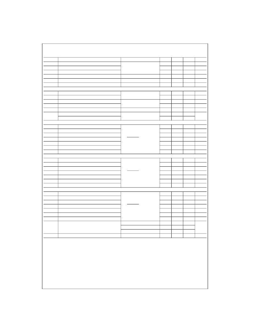
Transmitter AC Electrical Characteristics
Over supply voltage and operating temperature ranges, unless otherwise specified.
Note 12:
Outputs of all transmitters stay in 3-STATE until power reaches 2V. Both clock and data output begins to toggle 10ms after V
CC
reaches 3V and
Power-Down pin is above 1.5V.
Note 13:
This output data pulse position works for both transmitter with 21 TTL inputs except the LVDS output bit mapping difference (see Figure 15). Figure
16 shows the skew between the first data bit and clock output. Also 2-bit cycle delay is guaranteed when the MSB is output from transmitter.
Note 14:
This jitter specification is based on the assumption that PLL has a ref clock with cycle-to-cycle input jitter less than 2ns.
Symbol
t
TCP
t
TCH
t
TCL
t
CLKT
t
JIT
t
XIT
LVDS Transmitter Timing Characteristics
t
TLH
Differential Output Rise Time (20% to 80%)
t
THL
Differential Output Fall Time (80% to 20%)
t
STC
TxIn Setup to TxCLNIn
t
HTC
TxIn Holds to TCLKIn
t
TPDD
Transmitter Power-Down Delay
t
TCCD
Transmitter Clock Input to Clock Output Delay
Transmitter Clock Input to Clock Output Delay
Transmitter Output Data Jitter (f
=
40 MHz) (Note 13)
t
TPPB0
Transmitter Output Pulse Position of Bit 0
t
TPPB1
Transmitter Output Pulse Position of Bit 1
t
TPPB2
Transmitter Output Pulse Position of Bit 2
t
TPPB3
Transmitter Output Pulse Position of Bit 3
t
TPPB4
Transmitter Output Pulse Position of Bit 4
t
TPPB5
Transmitter Output Pulse Position of Bit 5
t
TPPB6
Transmitter Output Pulse Position of Bit 6
Transmitter Output Data Jitter (f
=
65 MHz) (Note 13)
t
TPPB0
Transmitter Output Pulse Position of Bit 0
t
TPPB1
Transmitter Output Pulse Position of Bit 1
t
TPPB2
Transmitter Output Pulse Position of Bit 2
t
TPPB3
Transmitter Output Pulse Position of Bit 3
t
TPPB4
Transmitter Output Pulse Position of Bit 4
t
TPPB5
Transmitter Output Pulse Position of Bit 5
t
TPPB6
Transmitter Output Pulse Position of Bit 6
Transmitter Output Data Jitter (f
=
85 MHz) (FIN1217 only) (Note 13)
t
TPPB0
Transmitter Output Pulse Position of Bit 0
t
TPPB1
Transmitter Output Pulse Position of Bit 1
t
TPPB2
Transmitter Output Pulse Position of Bit 2
t
TPPB3
Transmitter Output Pulse Position of Bit 3
t
TPPB4
Transmitter Output Pulse Position of Bit 4
t
TPPB5
Transmitter Output Pulse Position of Bit 5
t
TPPB6
Transmitter Output Pulse Position of Bit 6
t
JCC
FIN1217 Transmitter Clock Out Jitter
(Cycle-to-Cycle)
See Figure 19
Parameter
Test Conditions
Min
11.76
0.35
Typ
T
0.5
Max
50.0
0.65
Units
ns
T
Transmit Clock Period
Transmit Clock (TxCLKIn) HIGH Time
See Figure 6
Transmit Clock Low Time
TxCLKIn Transition Time (Rising and Failing)
TxCLKIn Cycle-to-Cycle Jitter
0.35
1.0
0.5
0.65
6.0
3.0
T
ns
ns
(10% to 90%) See Figure 7
TxIn Transition Time
1.5
6.0
ns
See Figure 4
0.75
1.5
ns
0.75
1.5
ns
ns
ns
See Figure 6
(f
=
85 MHz) (FIN1217 only)
See Figure 13, (Note 12)
See Figure 9
(T
A
=
25
°
C and with V
CC
=
3.3V)
2.5
0
100
5.5
6.8
ns
ns
2.8
See Figure 16
0.25
a
0.25
2a
0.25
3a
0.25
4a
0.25
5a
0.25
6a
0.25
0
a
0.25
a
+
0.25
2a
+
0.25
3a
+
0.25
4a
+
0.25
5a
+
0.25
6a
+
0.25
ns
ns
a
=
1
2a
3a
4a
ns
ns
ns
f x 7
5a
6a
ns
ns
See Figure 16
0.2
a
0.2
2a
0.2
3a
0.2
4a
0.2
5a
0.2
6a
0.2
0
a
2a
0.2
a
+
0.2
2a
+
0.2
3a
+
0.2
4a
+
0.2
5a
+
0.2
6a
+
0.2
ns
ns
ns
a
=
1
f x 7
3a
4a
5a
ns
ns
ns
6a
ns
See Figure 16
0.2
a
0.2
2a
0.2
3a
0.2
4a
0.2
5a
0.2
6a
0.2
0
0.2
a
+
0.2
2a
+
0.2
3a
+
0.2
4a
+
0.2
5a
+
0.2
6a
+
0.2
370
230
150
ns
a
2a
3a
ns
ns
ns
a
=
1
f x 7
4a
5a
6a
ns
ns
ns
f
=
40 MHz
f
=
65 MHz
f
=
85 MHz (FIN1217 only)
See Figure 11, (Note 13)
350
210
110
ps
t
TPLLS
Transmitter Phase Lock Loop Set Time (Note 14)
10.0
ms
相關PDF資料 |
PDF描述 |
|---|---|
| FIN1216MTD | LVDS 21-Bit Serializers/De-Serializers |
| FIN1217MTD | LVDS 21-Bit Serializers/De-Serializers |
| FIN1218 | LVDS 21-Bit Serializers/De-Serializers |
| FIN1218MTD | LVDS 21-Bit Serializers/De-Serializers |
| FIN12ACGFX | Low Voltage 12-Bit Bi-Directional Serializer/Deserializer with Multiple Frequency Ranges (Preliminary) |
相關代理商/技術參數 |
參數描述 |
|---|---|
| FIN1215MTD_Q | 功能描述:功率驅動器IC Serial/De-Serializer LVDS 21Bit RoHS:否 制造商:Micrel 產品:MOSFET Gate Drivers 類型:Low Cost High or Low Side MOSFET Driver 上升時間: 下降時間: 電源電壓-最大:30 V 電源電壓-最小:2.75 V 電源電流: 最大功率耗散: 最大工作溫度:+ 85 C 安裝風格:SMD/SMT 封裝 / 箱體:SOIC-8 封裝:Tube |
| FIN1215MTDX | 功能描述:LVDS 接口集成電路 Serial/De-Serializer LVDS 21Bit RoHS:否 制造商:Texas Instruments 激勵器數量:4 接收機數量:4 數據速率:155.5 Mbps 工作電源電壓:5 V 最大功率耗散:1025 mW 最大工作溫度:+ 85 C 封裝 / 箱體:SOIC-16 Narrow 封裝:Reel |
| FIN1215MTDX_NL | 制造商:FAIRCHILD 制造商全稱:Fairchild Semiconductor 功能描述:LVDS 21-Bit Serializers/De-Serializers |
| FIN1215MTDX_Q | 功能描述:LVDS 接口集成電路 Serial/De-Serializer LVDS 21Bit RoHS:否 制造商:Texas Instruments 激勵器數量:4 接收機數量:4 數據速率:155.5 Mbps 工作電源電壓:5 V 最大功率耗散:1025 mW 最大工作溫度:+ 85 C 封裝 / 箱體:SOIC-16 Narrow 封裝:Reel |
| FIN1216 | 制造商:FAIRCHILD 制造商全稱:Fairchild Semiconductor 功能描述:LVDS 21-Bit Serializers/De-Serializers |
發布緊急采購,3分鐘左右您將得到回復。