- 您現在的位置:買賣IC網 > PDF目錄375798 > FIN1216MTD (FAIRCHILD SEMICONDUCTOR CORP) LVDS 21-Bit Serializers/De-Serializers PDF資料下載
參數資料
| 型號: | FIN1216MTD |
| 廠商: | FAIRCHILD SEMICONDUCTOR CORP |
| 元件分類: | 通用總線功能 |
| 英文描述: | LVDS 21-Bit Serializers/De-Serializers |
| 中文描述: | TRIPLE LINE RECEIVER, PDSO48 |
| 封裝: | 6.10 MM, MO-153, TSSOP-48 |
| 文件頁數: | 9/17頁 |
| 文件大小: | 434K |
| 代理商: | FIN1216MTD |
9
www.fairchildsemi.com
F
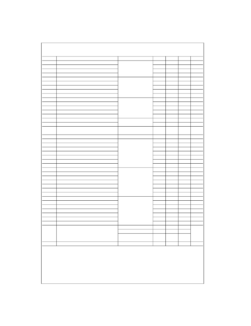
Receiver AC Electrical Characteristics
Over supply voltage and operating temperatures, unless otherwise specified
Note 17:
Receiver skew margin is defined as the valid sampling window after considering potential setup/hold time and minimum/maximum bit position.
Note 18:
Total channel latency from serializer to deserializer is (T
+
t
TCCD
)
+
(2*T
+
t
RCCD
). There is the clock period.
Symbol
t
RCOL
t
RCOH
t
RSRC
t
RHRC
t
RCOP
t
RCOL
t
RCOH
t
RSRC
t
RHRC
t
RCOP
t
RCOL
t
RCOH
t
RSRC
t
RHRC
t
ROLH
t
ROHL
t
RCCD
Parameter
Test Conditions
Min
10.0
10.0
Typ
11.0
12.2
Max
Units
ns
ns
RxCLKOut LOW Time
RxCLKOut HIGH Time
See Figure 8
RxOut Valid Prior to RxCLKOut
RxOut Valid After RxCLKOut
Receiver Clock Output (RxCLKOut) Period
(Rising Edge Strobe)
(f
=
40 MHz)
6.5
6.0
15.0
11.6
11.6
T
ns
ns
ns
50.0
RxCLKOut LOW Time
RxCLKOut HIGH Time
RxOut Valid Prior to RxCLKOut
See Figure 8
(Rising Edge Strobe)
(f
=
65 MHz)
5.0
5.0
4.5
7.8
7.3
7.7
9.0
9.0
ns
ns
ns
RxOut Valid After RxCLKOut
Receiver Clock Output (RxCLKOut) Period
RxCLKOut LOW Time
4.0
11.76
4.0
8.4
T
6.3
ns
ns
ns
50.0
6.0
See Figure 8
RxCLKOut HIGH Time
RxOut Valid Prior to RxCLKOut
RxOut Valid After RxCLKOut
(Rising Edge Strobe)
(f
=
85 MHz) (FIN1218 only)
4.5
3.5
3.5
5.4
6.3
6.5
6.5
ns
ns
ns
Output Rise Time (20% to 80%)
Output Fall Time (80% to 20%)
Receiver Clock Input to Clock Output Delay
C
L
=
8 pF
See Figure 5
See Figure 10 (Note 18)
T
A
=
25
°
C and V
CC
=
3.3V
See Figure 14
2.2
2.1
5.0
5.0
ns
ns
3.5
6.9
7.5
ns
t
RPDD
t
RSPB0
t
RSPB1
t
RSPB2
t
RSPB3
t
RSPB4
t
RSPB5
t
RSPB6
t
RSPB0
t
RSPB1
t
RSPB2
t
RSPB3
t
RSPB4
t
RSPB5
t
RSPB6
t
RSPB0
t
RSPB1
t
RSPB2
t
RSPB3
t
RSPB4
t
RSPB5
t
RSPB6
t
RSKM
Receiver Power-Down Delay
Receiver Input Strobe Position of Bit 0
1.0
2.15
μ
s
ns
1.0
Receiver Input Strobe Position of Bit 1
Receiver Input Strobe Position of Bit 2
Receiver Input Strobe Position of Bit 3
4.5
8.1
11.6
5.8
9.15
12.6
ns
ns
ns
See Figure 17
(f
=
40 MHz)
Receiver Input Strobe Position of Bit 4
Receiver Input Strobe Position of Bit 5
Receiver Input Strobe Position of Bit 6
15.1
18.8
22.5
16.3
19.9
23.6
ns
ns
ns
Receiver Input Strobe Position of Bit 0
Receiver Input Strobe Position of Bit 1
Receiver Input Strobe Position of Bit 2
0.7
2.9
5.1
1.4
3.6
5.8
ns
ns
ns
See Figure 17
(f
=
65 MHz)
Receiver Input Strobe Position of Bit 3
Receiver Input Strobe Position of Bit 4
Receiver Input Strobe Position of Bit 5
7.3
9.5
11.7
8.0
10.2
12.4
ns
ns
ns
Receiver Input Strobe Position of Bit 6
Receiver Input Strobe Position of Bit 0
Receiver Input Strobe Position of Bit 1
13.9
0.49
2.17
14.6
1.19
2.87
ns
ns
ns
Receiver Input Strobe Position of Bit 2
Receiver Input Strobe Position of Bit 3
Receiver Input Strobe Position of Bit 4
3.85
5.53
7.21
4.55
6.23
7.91
ns
ns
ns
See Figure 17
(f
=
85 MHz) (FIN1218 only)
Receiver Input Strobe Position of Bit 5
Receiver Input Strobe Position of Bit 6
RxIn Skew Margin
8.89
10.57
490
9.59
11.27
ns
ns
f
=
40 MHz; See Figure 18
f
=
65 MHz; See Figure 18
f
=
85 MHz (FIN1218 only);
See Figure 18
ps
(Note 17)
400
252
t
RPLLS
Receiver Phase Lock Loop Set Time
See Figure 12
10.0
ms
相關PDF資料 |
PDF描述 |
|---|---|
| FIN1217MTD | LVDS 21-Bit Serializers/De-Serializers |
| FIN1218 | LVDS 21-Bit Serializers/De-Serializers |
| FIN1218MTD | LVDS 21-Bit Serializers/De-Serializers |
| FIN12ACGFX | Low Voltage 12-Bit Bi-Directional Serializer/Deserializer with Multiple Frequency Ranges (Preliminary) |
| FIN12AC | Low Voltage 12-Bit Bi-Directional Serializer/Deserializer with Multiple Frequency Ranges (Preliminary) |
相關代理商/技術參數 |
參數描述 |
|---|---|
| FIN1216MTD_Q | 功能描述:功率驅動器IC LVDS 21-Bit RoHS:否 制造商:Micrel 產品:MOSFET Gate Drivers 類型:Low Cost High or Low Side MOSFET Driver 上升時間: 下降時間: 電源電壓-最大:30 V 電源電壓-最小:2.75 V 電源電流: 最大功率耗散: 最大工作溫度:+ 85 C 安裝風格:SMD/SMT 封裝 / 箱體:SOIC-8 封裝:Tube |
| FIN1216MTDX | 功能描述:LVDS 接口集成電路 LVDS 21-Bit RoHS:否 制造商:Texas Instruments 激勵器數量:4 接收機數量:4 數據速率:155.5 Mbps 工作電源電壓:5 V 最大功率耗散:1025 mW 最大工作溫度:+ 85 C 封裝 / 箱體:SOIC-16 Narrow 封裝:Reel |
| FIN1216MTDX_NL | 制造商:FAIRCHILD 制造商全稱:Fairchild Semiconductor 功能描述:LVDS 21-Bit Serializers/De-Serializers |
| FIN1217 | 制造商:FAIRCHILD 制造商全稱:Fairchild Semiconductor 功能描述:LVDS 21-Bit Serializers/De-Serializers |
| FIN1217_05 | 制造商:FAIRCHILD 制造商全稱:Fairchild Semiconductor 功能描述:LVDS 21-Bit Serializers/De-Serializers |
發布緊急采購,3分鐘左右您將得到回復。