- 您現(xiàn)在的位置:買賣IC網(wǎng) > PDF目錄375837 > FM1808-70-S (Electronic Theatre Controls, Inc.) 4Kb FRAM Serial 3V Memory PDF資料下載
參數(shù)資料
| 型號: | FM1808-70-S |
| 廠商: | Electronic Theatre Controls, Inc. |
| 元件分類: | DRAM |
| 英文描述: | 4Kb FRAM Serial 3V Memory |
| 中文描述: | 4Kb的鐵電串行3V的記憶 |
| 文件頁數(shù): | 6/12頁 |
| 文件大小: | 89K |
| 代理商: | FM1808-70-S |
Ramtron
FM1808-70
27 July 2000
6/12
FRAM Design Considerations
When designing with FRAM for the first time, users
of SRAM will recognize a few minor differences. First,
bytewide FRAM memories latch each address on the
falling edge of chip enable. This allows the address
bus to change after starting the memory access. Since
every access latches the memory address on the
falling edge of /CE, users should not ground it as they
might with SRAM.
Users that are modifying existing designs to use
FRAM should examine the hardware address
decoders. Decoders should be modified to qualify
addresses with an address valid signal if they do not
already. In many cases, this is the only change
required. Systems that drive chip enable active, then
inactive for each valid address may need no
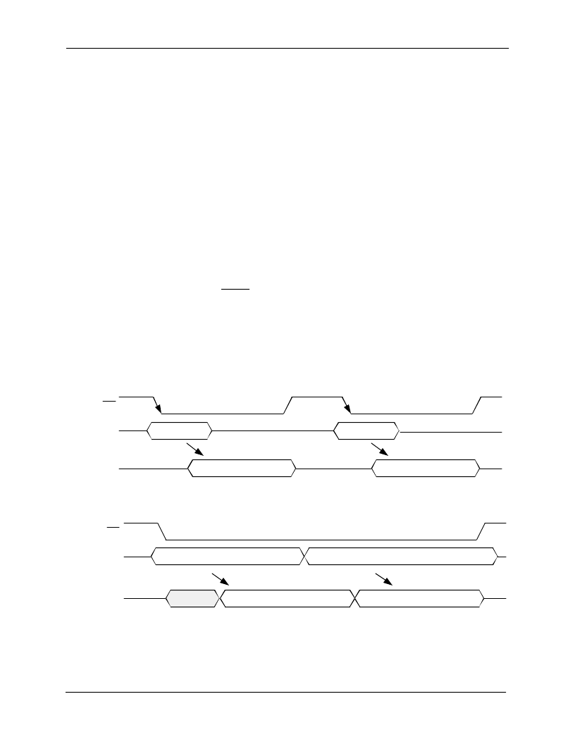
modifications. An example of the target signal
relationships are shown in Figure 4. Also shown is a
common SRAM signal relationship that will not work
for the FM1808.
Figure 4. Memory Address Relationships
The main design issue is to create a decoder scheme
that will drive /CE active, then inactive for each
address. This accomplishes the two goals of latching
the new address and creating the precharge period.
A second design consideration relates to the level of
VDD during operation. Battery-backed SRAMs are
forced to monitor VDD in order to switch to battery
backup. They typically block user access below a
certain VDD level in order to prevent loading the
battery with current demand from an active SRAM.
The user can be abruptly cut off from access to the
nonvolatile memory in a power down situation with
no warning or indication.
FRAM memories do not need this system overhead.
The memory will not block access at any VDD level.
The user, however, should prevent the processor
from accessing memory when VDD is out-of-
tolerance. The common design practice of holding a
processor in reset when VDD drops is adequate; no
special provisions must be taken for FRAM design.
Valid Memory Read Relationship
FRAM
Signaling
CE
Address
A1
A2
Data
D1
D2
Invalid Memory Read Relationship
SRAM
Signaling
CE
Address
A1
A2
Data
D1
D2
相關(guān)PDF資料 |
PDF描述 |
|---|---|
| FM200TU-07A | HIGH POWER SWITCHING USE INSULATED PACKAGE |
| FM200TU-2A | HIGH POWER SWITCHING USE INSULATED PACKAGE |
| FM200TU-3A | HIGH POWER SWITCHING USE INSULATED PACKAGE |
| FM20L08 | 1Mbit Bytewide FRAM Memory ? Extended Temp |
| FM20L08-60-TG | 1Mbit Bytewide FRAM Memory ? Extended Temp |
相關(guān)代理商/技術(shù)參數(shù) |
參數(shù)描述 |
|---|---|
| FM1808-70-SG | 功能描述:F-RAM 256K (32Kx8) 70ns 5V RoHS:否 存儲容量:512 Kbit 組織:64 K x 8 接口:SPI 工作電源電壓:2 V to 3.6 V 工作溫度范圍:- 40 C to + 85 C 安裝風(fēng)格:SMD/SMT 封裝 / 箱體:SOIC-8 封裝:Tube 制造商:Cypress Semiconductor |
| FM1808-70-SG | 制造商:Ramtron International Corporation 功能描述:Nonvolatile SRAM Memory IC Memory Type:F |
| FM1808-70-SGTR | 功能描述:F-RAM 256K (32Kx8) 70ns 5V RoHS:否 存儲容量:512 Kbit 組織:64 K x 8 接口:SPI 工作電源電壓:2 V to 3.6 V 工作溫度范圍:- 40 C to + 85 C 安裝風(fēng)格:SMD/SMT 封裝 / 箱體:SOIC-8 封裝:Tube 制造商:Cypress Semiconductor |
| FM1808-70-STR | 功能描述:F-RAM 256K (32Kx8) 70ns 5V RoHS:否 存儲容量:512 Kbit 組織:64 K x 8 接口:SPI 工作電源電壓:2 V to 3.6 V 工作溫度范圍:- 40 C to + 85 C 安裝風(fēng)格:SMD/SMT 封裝 / 箱體:SOIC-8 封裝:Tube 制造商:Cypress Semiconductor |
| FM1808B | 制造商:RAMTRON 制造商全稱:RAMTRON 功能描述:256Kb Bytewide 5V F-RAM Memory |
發(fā)布緊急采購,3分鐘左右您將得到回復(fù)。