- 您現在的位置:買賣IC網 > PDF目錄375846 > FM24C32U (Fairchild Semiconductor Corporation) 32K-Bit Standard 2-Wire Bus Interface Serial EEPROM PDF資料下載
參數資料
| 型號: | FM24C32U |
| 廠商: | Fairchild Semiconductor Corporation |
| 英文描述: | 32K-Bit Standard 2-Wire Bus Interface Serial EEPROM |
| 中文描述: | 32K的位標準2線總線接口的串行EEPROM |
| 文件頁數: | 7/13頁 |
| 文件大小: | 85K |
| 代理商: | FM24C32U |
7
www.fairchildsemi.com
FM24C32U Rev. A.1
F
Background Information (IIC Bus)
Extended IIC specification is an extension of Standard IIC speci-
fication to allow addressing of EEPROMs with more than 16Kbits
of memory on an IIC bus. The difference between the two
specifications is that Extended IIC specification defines two bytes
of
“
Array Address
”
information while Standard IIC specification
defines only one. All other aspects are identical between the two
specifications. Using two bytes of Array Address and 3 address
signals (A2, A1 and A0), it is now possible to address up to 4 Mbits
(2
8
* 2
8
* 2
3
* 8 = 4 Mbits) of memory on an IIC bus.
Note that due to format difference, it is not possible to have
peripherals which follow Standard IIC specification (e.g. 16K bit
EEPROM) and peripherals which follow Extended IIC specifica-
tion (e.g. 32K bit EEPROM) on a common IIC bus.
IIC bus allows synchronous bi-directional communication be-
tween a TRANSMITTER and a RECEIVER using a Clock signal
(SCL) and a Data signal (SDA). Additionally there are up to three
Address signals (A2, A1 and A0) which collectively serve as
“
chip
select signal
”
to a device (e.g. EEPROM) on the bus.
All communication on the IIC bus must be started with a valid
START condition (by a MASTER), followed by transmittal (by the
MASTER) of byte(s) of information (Address/Data). For every
byte of information received, the addressed RECEIVER provides
a valid ACKNOWLEDGE pulse to further continue the communi-
cation unless the RECEIVER intends to discontinue the commu-
nication. Depending on the direction of transfer (Write or Read),
the RECEIVER can be a SLAVE or the MASTER. A typical IIC
communication concludes with a STOP condition (by the MAS-
TER).
Addressing an EEPROM memory location involves sending a
command string with the following information:
[DEVICE TYPE]
—
[DEVICE/PAGE BLOCK SELECTION]
—
[R/W
BIT]
—
[ARRAY ADDRESS#1]
—
[ARRAY ADDRESS#0]
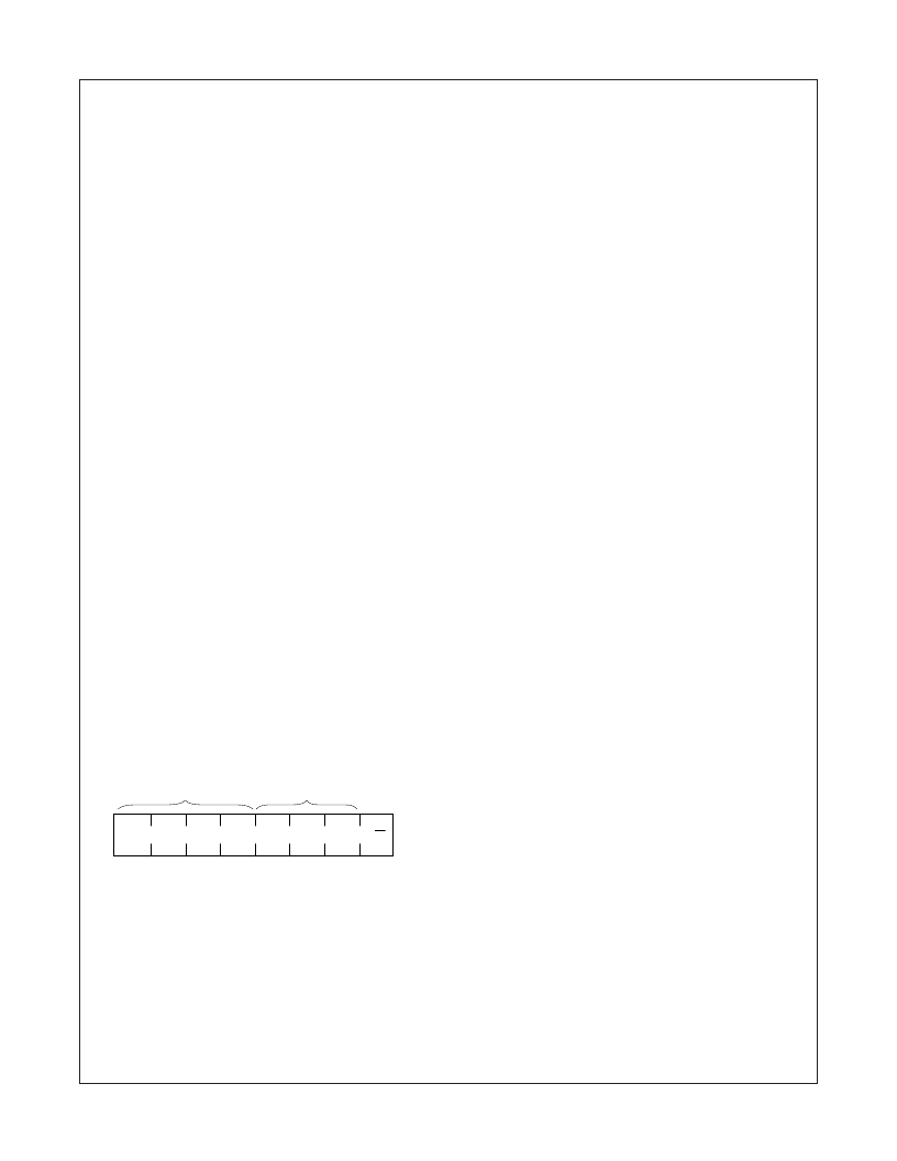
Slave Address
Slave Address is an 8-bit information consisting of a Device type
field (4bits), Device/Page block selection field (3bits) and Read/
Write bit (1bit).
Slave Address Format
Device Type
IIC bus is designed to support a variety of devices such as RAMs,
EPROMs etc., along with EEPROMS. Hence to properly identify
various devices on the IIC bus, a 4-bit
“
Device Type
”
identifier
string is used. For EEPROMS, this 4-bit string is 1-0-1-0. Every IIC
device on the bus internally compares this 4-bit string to its own
“
Device Type
”
string to ensure proper device selection.
Device/Page Block Selection
When multiple devices of the same type (e.g. multiple EEPROMS)
are present on the IIC bus, then the A2, A1 and A0 address
information bits are used in device selection. Every IIC device on
the bus internally compares this 3-bit string to its own physical
configuration (A2, A1 and A0 pins) to ensure proper device
selection. This comparison is in addition to the
“
Device Type
”
comparison.
In addition to selecting an EEPROM, these 3 bits are also used to
select a
“
page block
”
within the selected EEPROM. Each page
block is 512Kbit (64 K Bytes) in size. If an EEPROM contains more
than one page bock then the selection of a page block within the
EEPROM is by using A2, A1 and A0 bits.
Read/Write Bit
Last bit of the Slave Address indicates if the intended access is
Read or Write. If the bit is "1," then the access is Read, whereas
if the bit is "0," then the access is Write.
Acknowledge
Acknowledge is an active LOW pulse on the SDA line driven by an
addressed receiver to the addressing transmitter to indicate
receipt of 8-bits of data. The receiver provides an ACK pulse for
every 8-bits of data received. This handshake mechanism is done
as follows: After transmitting 8-bits of data, the transmitter re-
leases the SDA line and waits for the ACK pulse. The addressed
receiver, if present, drives the ACK pulse on the SDA line during
the 9th clock and releases the SDA line back (to the transmitter).
Refer Figure 3.
Array Address#1
This is an 8-bit information containing the most significant 8-bits of
16-bit memory array address of a location to be selected within a
page block of the device.
Array Address#0
This is an 8-bit information containing the least significant 8-bits of
16-bit memory array address of a location to be selected within a
page block of the device.
Device Type
Identifier
Device/Page Block
Selection
1
0
1
0
A2
A1
A0
R/W
(LSB)
相關PDF資料 |
PDF描述 |
|---|---|
| FM24C32UFTEM8 | EEPROM |
| FM24C32UFTEN | EEPROM |
| FM24C32UFTHEM8 | EEPROM |
| FM24C32UFTHEN | EEPROM |
| FM24C32UFTHM8 | EEPROM |
相關代理商/技術參數 |
參數描述 |
|---|---|
| FM24C32UEM8 | 功能描述:電可擦除可編程只讀存儲器 USE 511-M24C32-MN6 RoHS:否 制造商:Atmel 存儲容量:2 Kbit 組織:256 B x 8 數據保留:100 yr 最大時鐘頻率:1000 KHz 最大工作電流:6 uA 工作電源電壓:1.7 V to 5.5 V 最大工作溫度:+ 85 C 安裝風格:SMD/SMT 封裝 / 箱體:SOIC-8 |
| FM24C32UEM8X | 功能描述:電可擦除可編程只讀存儲器 DISC BY MFG 7/03 RoHS:否 制造商:Atmel 存儲容量:2 Kbit 組織:256 B x 8 數據保留:100 yr 最大時鐘頻率:1000 KHz 最大工作電流:6 uA 工作電源電壓:1.7 V to 5.5 V 最大工作溫度:+ 85 C 安裝風格:SMD/SMT 封裝 / 箱體:SOIC-8 |
| FM24C32UEN | 制造商:Fairchild Semiconductor Corporation 功能描述: |
| FM24C32UFEM8 | 功能描述:電可擦除可編程只讀存儲器 RoHS:否 制造商:Atmel 存儲容量:2 Kbit 組織:256 B x 8 數據保留:100 yr 最大時鐘頻率:1000 KHz 最大工作電流:6 uA 工作電源電壓:1.7 V to 5.5 V 最大工作溫度:+ 85 C 安裝風格:SMD/SMT 封裝 / 箱體:SOIC-8 |
| FM24C32UFEM8X | 功能描述:電可擦除可編程只讀存儲器 DISC BY MFG 7/03 RoHS:否 制造商:Atmel 存儲容量:2 Kbit 組織:256 B x 8 數據保留:100 yr 最大時鐘頻率:1000 KHz 最大工作電流:6 uA 工作電源電壓:1.7 V to 5.5 V 最大工作溫度:+ 85 C 安裝風格:SMD/SMT 封裝 / 箱體:SOIC-8 |
發布緊急采購,3分鐘左右您將得到回復。