- 您現(xiàn)在的位置:買賣IC網(wǎng) > PDF目錄375849 > FM31256-S (Electronic Theatre Controls, Inc.) Integrated Processor Companion with Memory PDF資料下載
參數(shù)資料
| 型號: | FM31256-S |
| 廠商: | Electronic Theatre Controls, Inc. |
| 英文描述: | Integrated Processor Companion with Memory |
| 中文描述: | 綜合處理器與記憶體伴侶 |
| 文件頁數(shù): | 14/22頁 |
| 文件大小: | 286K |
| 代理商: | FM31256-S |
Start Condition
A Start condition is indicated when the bus master
drives SDA from high to low while the SCL signal is
high. All read and write transactions begin with a
Start condition. An operation in progress can be
aborted by asserting a Start condition at any time.
Aborting an operation using the Start condition will
ready the FM31xxx for a new operation.
If the power supply drops below the specified VTP
during operation, any 2-wire transaction in progress
will be aborted and the system must issue a Start
condition prior to performing another operation.
FM3104/16/64/256
Rev 0.2
May 2003
Page 14 of 22
Stop Condition
A Stop condition is indicated when the bus master
drives SDA from low to high while the SCL signal is
high. All operations must end with a Stop condition.
If an operation is pending when a stop is asserted,
the operation will be aborted. The master must have
control of SDA (not a memory read) in order to
assert a Stop condition.
Data/Address Transfer
All data transfers (including addresses) take place
while the SCL signal is high. Except under the two
conditions described above, the SDA signal should
not change while SCL is high.
Acknowledge
The Acknowledge (ACK) takes place after the 8
th
data bit has been transferred in any transaction.
During this state the transmitter must release the
SDA bus to allow the receiver to drive it. The
receiver drives the SDA signal low to acknowledge
receipt of the byte. If the receiver does not drive
SDA low, the condition is a No-Acknowledge
(NACK) and the operation is aborted.
The receiver might NACK for two distinct reasons.
First is that a byte transfer fails. In this case, the
NACK ends the current operation so that the part can
be addressed again. This allows the last byte to be
recovered in the event of a communication error.
Second and most common, the receiver does not
send an ACK to deliberately terminate an operation.
For example, during a read operation, the FM31xxx
will continue to place data onto the bus as long as the
receiver sends ACKs (and clocks). When a read
operation is complete and no more data is needed,
the receiver must NACK the last byte. If the receiver
ACKs the last byte, this will cause the FM31xxx to
attempt to drive the bus on the next clock while the
master is sending a new command such as a Stop.
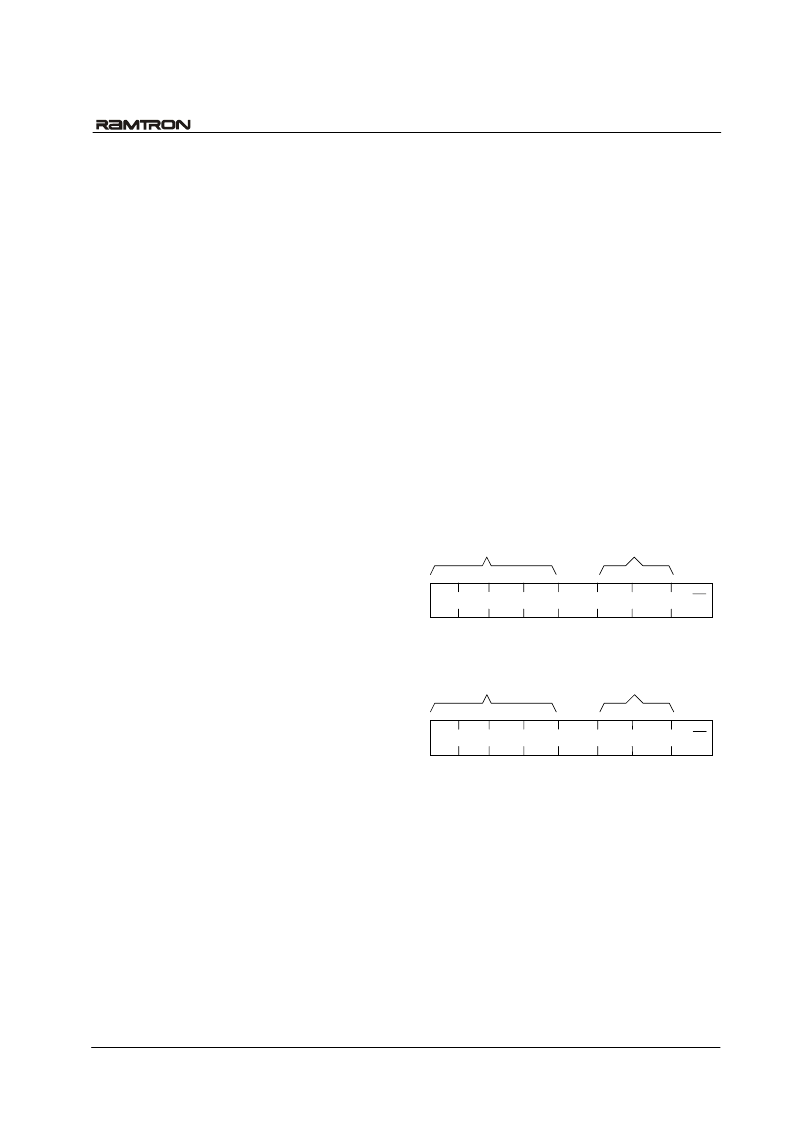
Slave Address
The first byte that the FM31xxx expects after a Start
condition is the slave address. As shown in figures
below, the slave address contains the Slave ID,
Device Select address, and a bit that specifies if the
transaction is a read or a write.
The FM31xxx has two Slave Addresses (Slave IDs)
associated with two logical devices. To access the
memory device, bits 7-4 should be set to 1010b. The
other logical device within the FM31xxx is the real-
time clock and companion. To access this device,
bits 7-4 of the slave address should be set to 1101b.
A bus transaction with this slave address will not
affect the memory in any way. The figures below
illustrate the two Slave Addresses.
The Device Select bits allow multiple devices of the
same type to reside on the 2-wire bus. The device
select bits (bits 2-1) select one of four parts on a two-
wire bus. They must match the corresponding value
on the external address pins in order to select the
device. Bit 0 is the read/write bit. A “1” indicates a
read operation, and a “0” indicates a write operation.
1
0
1
0
X
A1
A0
R/W
Slave ID
Device
Select
7
6
5
4
3
2
1
0
Figure 9. Slave Address - Memory
Figure 10. Slave Address – Companion
Addressing Overview – Memory
After the FM31xxx acknowledges the Slave
Address, the master can place the memory address
on the bus for a write operation. The address requires
two bytes. This is true for all members of the family.
Therefore the 4Kb and 16Kb configurations will be
addressed differently from stand alone serial
memories but the entire family will be upwardly
compatible with no software changes.
The first is the MSB (upper byte). For a given
density unused address bits are don’t cares, but
should be set to 0 to maintain upward compatibility.
1
1
0
1
X
A1
A0
R/W
Slave ID
7
6
5
4
3
2
1
0
Device
Select
相關PDF資料 |
PDF描述 |
|---|---|
| FM3164-S | Integrated Processor Companion with Memory |
| FM3204 | Integrated Processor Companion with Memory |
| FM3204-G | Integrated Processor Companion with Memory |
| FM3204-S | Integrated Processor Companion with Memory |
| FM3216 | Integrated Processor Companion with Memory |
相關代理商/技術參數(shù) |
參數(shù)描述 |
|---|---|
| FM31256-STR | 功能描述:監(jiān)控電路 256K w/RTC Pwr Mon WDT Bat Sw PF RoHS:否 制造商:STMicroelectronics 監(jiān)測電壓數(shù): 監(jiān)測電壓: 欠電壓閾值: 過電壓閾值: 輸出類型:Active Low, Open Drain 人工復位:Resettable 監(jiān)視器:No Watchdog 電池備用開關:No Backup 上電復位延遲(典型值):10 s 電源電壓-最大:5.5 V 最大工作溫度:+ 85 C 安裝風格:SMD/SMT 封裝 / 箱體:UDFN-6 封裝:Reel |
| FM31272 | 制造商:RAMTRON 制造商全稱:RAMTRON 功能描述:5V Integrated Processor Companion with Memory |
| FM31272-G | 功能描述:F-RAM 4K w/RTC Pwr Mon WDT Bat Sw PF RoHS:否 存儲容量:512 Kbit 組織:64 K x 8 接口:SPI 工作電源電壓:2 V to 3.6 V 工作溫度范圍:- 40 C to + 85 C 安裝風格:SMD/SMT 封裝 / 箱體:SOIC-8 封裝:Tube 制造商:Cypress Semiconductor |
| FM31272-GTR | 功能描述:F-RAM 4K w/RTC Pwr Mon WDT Bat Sw PF RoHS:否 存儲容量:512 Kbit 組織:64 K x 8 接口:SPI 工作電源電壓:2 V to 3.6 V 工作溫度范圍:- 40 C to + 85 C 安裝風格:SMD/SMT 封裝 / 箱體:SOIC-8 封裝:Tube 制造商:Cypress Semiconductor |
| FM31274 | 制造商:RAMTRON 制造商全稱:RAMTRON 功能描述:5V Integrated Processor Companion with Memory |
發(fā)布緊急采購,3分鐘左右您將得到回復。