- 您現在的位置:買賣IC網 > PDF目錄375849 > FM3264-S (Electronic Theatre Controls, Inc.) Integrated Processor Companion with Memory PDF資料下載
參數資料
| 型號: | FM3264-S |
| 廠商: | Electronic Theatre Controls, Inc. |
| 英文描述: | Integrated Processor Companion with Memory |
| 中文描述: | 綜合處理器與記憶體伴侶 |
| 文件頁數: | 17/20頁 |
| 文件大小: | 285K |
| 代理商: | FM3264-S |
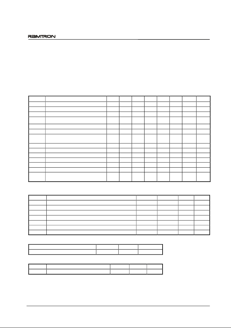
Notes
1.
SCL toggling between V
DD
-0.3V and V
SS
, other inputs V
SS
or V
DD
-0.3V.
2.
All inputs at V
SS
or V
DD,
static. Stop command issued.
3.
V
IN
or V
OUT
= V
SS
to V
DD
. Does not apply to A0, A1, PFI, or /RST pins.
4.
V
BAK
= 3.0V, V
DD
< 2.4V, CNT1-2 at V
BAK
.
5.
/RST is asserted low when V
DD
< V
TP
.
6.
The minimum V
DD
to guarantee the level of /RST remains a valid V
OL
level.
7.
Full complete operation. Supervisory circuits operate to lower voltages as specified.
8.
Includes /RST input detection of external reset condition to trigger driving of /RST signal by FM32xx.
9.
The VBAK trickle charger automatically regulates the maximum voltage on this pin for capacitor backup applications.
10.
V
BAK
will source current when trickle charge is enabled (VBC bit=1), V
DD
> V
BAK
, and V
BAK
< V
BAK
max.
AC Parameters
(T
A
= -40
°
C to + 85
°
C, V
DD
= 2.7V to 5.5V, C
L
= 100 pF unless otherwise specified)
Symbol Parameter
Min
f
SCL
SCL Clock Frequency
0
t
LOW
Clock Low Period
4.7
t
HIGH
Clock High Period
4.0
t
AA
SCL Low to SDA Data Out Valid
FM3204/16/64/256
Rev 2.1
Dec. 2004
Page 17 of 20
Max
100
3
Min
0
1.3
0.6
Max
400
0.9
Min
0
0.6
0.4
Max
1000
0.55
Units
kHz
μ
s
μ
s
μ
s
Notes
t
BUF
t
HD:STA
t
SU:STA
Bus Free Before New Transmission
Start Condition Hold Time
Start Condition Setup for Repeated
Start
Data In Hold Time
Data In Setup Time
Input Rise Time
Input Fall Time
Stop Condition Setup Time
Data Output Hold
(from SCL @ VIL)
Noise Suppression Time Constant
on SCL, SDA
All SCL specifications as well as start and stop conditions apply to both read and write operations.
Supervisor Timing
(T
A
= -40
°
C to + 85
°
C, V
DD
= 2.7V to 5.5V)
Symbol
Parameter
t
RPU
Reset active after V
DD
>V
TP
t
RNR
V
DD
< V
TP
noise immunity
t
VR
V
DD
Rise Time
t
VF
V
DD
Fall Time
t
WDP
Pulse Width of /RST for Watchdog Reset
t
WDOG
Timeout of Watchdog
f
CNT
Frequency of Event Counters
Data Retention
(T
A
= -40
°
C to + 85
°
C, V
DD
= 2.7V to 5.5V)
Parameter
Data Retention
Capacitance
(T
A
= 25
°
C, f=1.0 MHz, V
DD
= 3.0V)
Symbol
Parameter
C
IO
Input/output capacitance
Notes
1
This parameter is characterized but not tested.
2
Slope measured at any point on V
DD
waveform.
3
t
DOG
is the programmed time in register 0Ah, V
DD
> V
TP
and t
RPU
satisfied.
4.7
4.0
4.7
1.3
0.6
0.6
0.5
0.25
0.25
μ
s
μ
s
μ
s
t
HD:DAT
t
SU:DAT
t
R
t
F
t
SU:STO
t
DH
t
SP
0
0
0
ns
ns
ns
ns
μ
s
ns
ns
250
4.0
0
100
0.6
0
100
0.25
0
1000
300
50
300
300
50
300
100
50
1
1
Min
100
10
50
100
100
t
DOG
0
Max
200
25
-
-
200
2*t
DOG
10
Units
ms
μ
s
μ
s/V
μ
s/V
ms
ms
MHz
Notes
1
1,2
1,2
3
Min
10
Units
Years
Notes
Max
8
Units
pF
Notes
1
相關PDF資料 |
PDF描述 |
|---|---|
| FM34W02ULZ | RoHS Compliant:Yes RoHS Compliant: Yes |
| FM34W02UEM8 | I2C Serial EEPROM |
| FM34W02UEMT8 | I2C Serial EEPROM |
| FM34W02ULEM8 | I2C Serial EEPROM |
| FM34W02ULEMT8 | I2C Serial EEPROM |
相關代理商/技術參數 |
參數描述 |
|---|---|
| FM3264-STR | 功能描述:監控電路 64K w/Pwr Mon WDT Bat Sw Pwr Fail RoHS:否 制造商:STMicroelectronics 監測電壓數: 監測電壓: 欠電壓閾值: 過電壓閾值: 輸出類型:Active Low, Open Drain 人工復位:Resettable 監視器:No Watchdog 電池備用開關:No Backup 上電復位延遲(典型值):10 s 電源電壓-最大:5.5 V 最大工作溫度:+ 85 C 安裝風格:SMD/SMT 封裝 / 箱體:UDFN-6 封裝:Reel |
| FM32L272 | 制造商:RAMTRON 制造商全稱:RAMTRON 功能描述:3V Integrated Processor Companion with Memory |
| FM32L272-G | 功能描述:F-RAM 4K w/Pwr Mon WDT Bat Sw PF Ser Num RoHS:否 存儲容量:512 Kbit 組織:64 K x 8 接口:SPI 工作電源電壓:2 V to 3.6 V 工作溫度范圍:- 40 C to + 85 C 安裝風格:SMD/SMT 封裝 / 箱體:SOIC-8 封裝:Tube 制造商:Cypress Semiconductor |
| FM32L272-GTR | 功能描述:F-RAM 4K w/Pwr Mon WDT Bat Sw PF Ser Num RoHS:否 存儲容量:512 Kbit 組織:64 K x 8 接口:SPI 工作電源電壓:2 V to 3.6 V 工作溫度范圍:- 40 C to + 85 C 安裝風格:SMD/SMT 封裝 / 箱體:SOIC-8 封裝:Tube 制造商:Cypress Semiconductor |
| FM32L274 | 制造商:RAMTRON 制造商全稱:RAMTRON 功能描述:3V Integrated Processor Companion with Memory |
發布緊急采購,3分鐘左右您將得到回復。