- 您現(xiàn)在的位置:買賣IC網(wǎng) > PDF目錄375852 > FM573-P (Electronic Theatre Controls, Inc.) Nonvolatile Octal Latch/Register PDF資料下載
參數(shù)資料
| 型號: | FM573-P |
| 廠商: | Electronic Theatre Controls, Inc. |
| 英文描述: | Nonvolatile Octal Latch/Register |
| 中文描述: | 非易失八進(jìn)制鎖存/注冊 |
| 文件頁數(shù): | 7/10頁 |
| 文件大小: | 94K |
| 代理商: | FM573-P |
Ramtron
FM573/574
27 March 2001
7/10
AC Parameters
TA = -40
°
C to + 85
°
C, CL = 50 pF unless otherwise specified
Symbol
Parameter
f
MAX
Maximum clock frequency
t
CW
Clock minimum pulse width
t
PD
Propagation delay Dn to Qn
Propagation delay C to Qn
t
EN
Output enable time /OE to Qn
t
DIS
Output disable /OE to Qn Hi-Z
t
DS
Data setup Dn to C low (573)
Data setup Dn to C
↑
(574)
t
DH
Data hold Dn after C low (573)
Data hold after C high (574)
Notes:
1
This parameter is characterized but not tested.
Power Cycling and Data Retention
TA = -40
°
C to + 85
°
C, VDD = 2.7V to 5.5V unless otherwise specified
VDD=2.7V – 3.6V
Symbol
Parameter
Min
Nonvolatile data retention
1
Latched state changes
1E10
t
PDS
Last state change to V
MIN
2
t
RES
V
MIN
to output valid
t
PUH
V
MIN
to first user write
1.5
Notes:
1. Data retention is measured from the last state change, and is the time that a state will be retained at 85
°
C and
correctly restored on power-up. The process of powering up (and reading the nonvolatile state) refreshes the
stored state and re-starts the data retention period even if the state is unchanged.
2. The nonvolatile elements are written when the latched state changes. Changes on either Dn or Qn that are not
latched have no effect.
3. The last write to the nonvolatile latch element must occur prior to reaching V
MIN
during a power down.
4. After the power supply reaches approximately V
MIN
during a power up, the nonvolatile latch is read and the
value restored to the user latch. This spec. provides the time needed to restore the FM573/FM574 pins to the
restored state depending on the state of /OE.
5. The user should not attempt to write during the restore process. In particular, powering up in transparent mode
(FM573) defeats the purpose of using a nonvolatile latch.
Capacitance
TA = 25
°
C , f=1.0 MHz, VDD = 5V
Symbol
Parameter
Max
C
IN
Input capacitance
6
Notes
1
This parameter is characterized but not tested.
AC Test Conditions
Input Pulse Levels
0.1VDD to 0.9VDD
Input rise and fall times
10 ns
Input and output timing levels
0.3VDD, 0.7 VDD
VDD=2.7V – 3.6V
Min
VDD=5.0V +/- 10%
Min
30
8
Max
Max
Units
MHz
ns
ns
Notes
30
12
80
33
5
70
60
5
28
25
ns
ns
ns
1
7
5
ns
VDD=5.0V +/- 10%
Min
1
1E10
1
1.5
Max
Max
Units
Year
Changes
μ
S
μ
S
μ
S
Notes
1
2
3
4
4,5
1
1
Units
pF
Notes
1
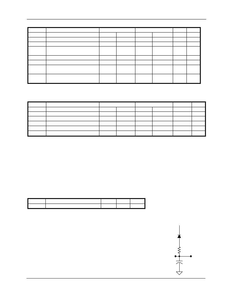
Equivalent AC Load Circuit
1.3V
Output
3300
50 pF
相關(guān)PDF資料 |
PDF描述 |
|---|---|
| FM574-P | Nonvolatile Octal Latch/Register |
| FM574-S | Nonvolatile Octal Latch/Register |
| FM573 | Nonvolatile Octal Latch/Register |
| FM574 | Nonvolatile Octal Latch/Register |
| FM573-S | Nonvolatile Octal Latch/Register |
相關(guān)代理商/技術(shù)參數(shù) |
參數(shù)描述 |
|---|---|
| FM573-S | 制造商:未知廠家 制造商全稱:未知廠家 功能描述:Nonvolatile Octal Latch/Register |
| FM574 | 制造商:Black Box Corporation 功能描述:RCA A/V SOLDER TYPE MOD OW AV MOD GIGASTATION+ |
| FM574-P | 制造商:未知廠家 制造商全稱:未知廠家 功能描述:Nonvolatile Octal Latch/Register |
| FM574-S | 制造商:未知廠家 制造商全稱:未知廠家 功能描述:Nonvolatile Octal Latch/Register |
| FM575 | 制造商:Black Box Corporation 功能描述:RCA A/V GOLD F/F FEEDTHR OW AV MOD GIGASTATION+ |
發(fā)布緊急采購,3分鐘左右您將得到回復(fù)。