- 您現(xiàn)在的位置:買(mǎi)賣(mài)IC網(wǎng) > PDF目錄375852 > FM573 (Electronic Theatre Controls, Inc.) Nonvolatile Octal Latch/Register PDF資料下載
參數(shù)資料
| 型號(hào): | FM573 |
| 廠商: | Electronic Theatre Controls, Inc. |
| 英文描述: | Nonvolatile Octal Latch/Register |
| 中文描述: | 非易失八進(jìn)制鎖存/注冊(cè) |
| 文件頁(yè)數(shù): | 6/10頁(yè) |
| 文件大小: | 94K |
| 代理商: | FM573 |
Ramtron
FM573/574
27 March 2001
6/10
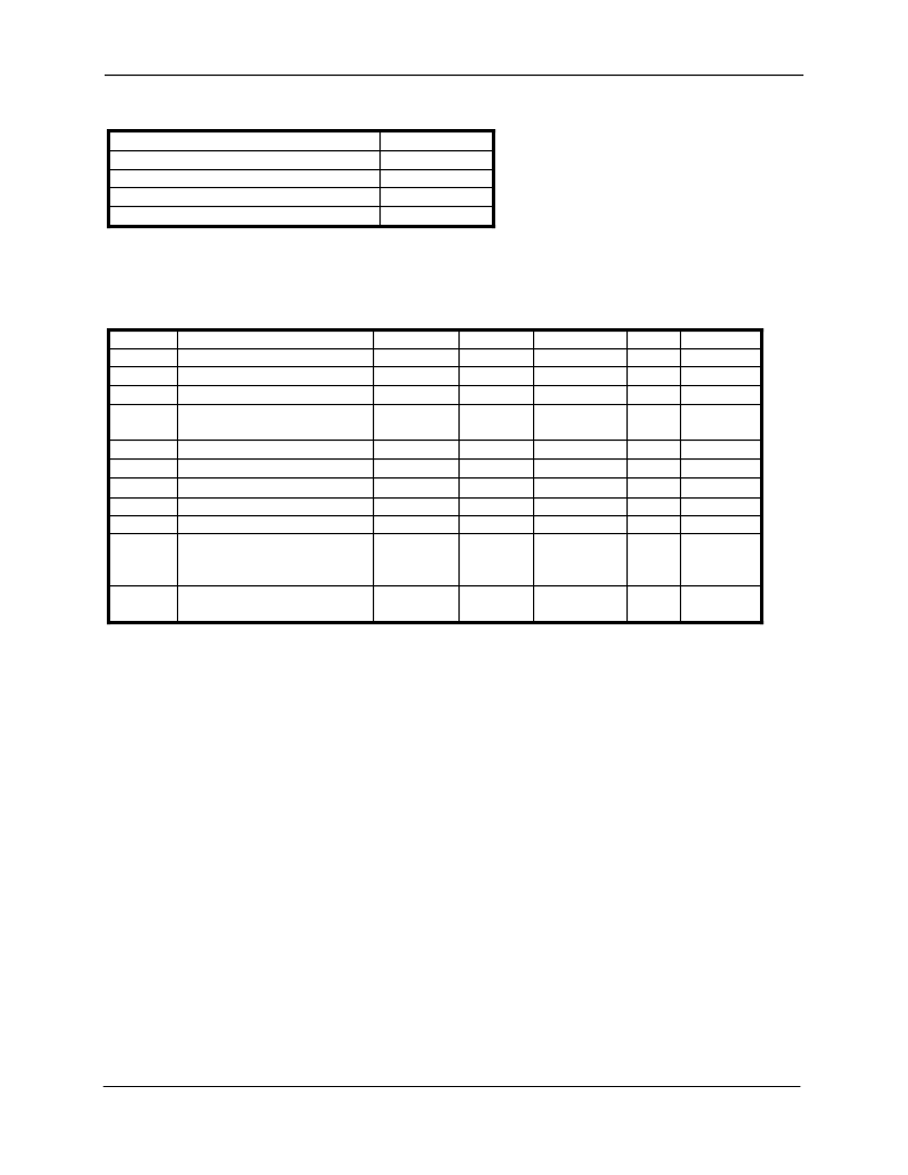
Electrical Specifications
Absolute Maximum Ratings
Description
Ratings
-40
°
C to + 85
°
C
-1.0V to +7.0V
TBD
300
°
C
Ambient storage or operating temperature
Voltage on any pin with respect to ground
D.C. output current on any pin
Lead temperature (Soldering, 10 seconds)
Stresses above those listed under Absolute Maximum Ratings may cause permanent damage to the device. This is a
stress rating only, and the functional operation of the device at these or any other conditions above those listed in the
operational section of this specification is not implied. Exposure to absolute maximum ratings conditions for
extended periods may affect device reliability.
DC Operating Conditions
TA = -40
°
C to + 85
°
C, VDD = 2.7V to 5.5V unless otherwise specified
Symbol
Parameter
Min
V
DD
Main Power Supply
2.7
V
MIN
State change blocked/restored 2.40
I
SB
Quiescent Supply Current
I
DDDY
Dynamic Supply Current
ex. 3.3V, 10 MHz, 8 inputs
I
DDNV
State Change Supply Current
I
LI
Input Leakage Current
I
LO
Output Leakage Current
V
IL
Input Low Voltage
-0.3
V
IH
Input High Voltage
0.7*VDD
V
OH
Output High Voltage
@ IOH = -8 mA VDD>4V
@ IOH = -8 mA VDD<4V
VDD-1.0
V
OL
Output Low Voltage
@ IOL = 8 mA
Notes
1. Referenced to VSS.
2. C = VSS, all other inputs at VDD or VSS
3. Dynamic supply current depends on the clock frequency, the frequency of inputs toggling, and the number of
bits toggling. In the formula, V = VDD; f is clock frequency; n is the number of bits switching. The Dn inputs
toggle at approximately a 50% duty-cycle at of the frequency of C and comply with the minimum setup time.
Outputs are tri-stated. All input levels at VDD and VSS. If C is static but the inputs toggle (573 in transparent
mode), then the f should be the frequency of the inputs.
4. In a realistic system, the IDD needed to drive the loads also should be considered. I
L
= C
L
*V*f
o
*n where C
L
is
the load capacitance, V is the output swing voltage, f
o
is the output frequency, and n is the number of bits
switching.
5. Changes in state cause a nonvolatile write which adds a DC current component to the static power or dynamic
for the duration of the nonvolatile write operation. The total current consumption after each state change = I
SB
+
I
DDNV
+ I
DDDY
. After the state change is recorded, total current consumption = I
SB
+ I
DDDY.
6. VIN or VOUT = VSS to VDD
7. This parameter is characterized but not tested.
8. All state changes will be ignored when VDD is below V
MIN
. VDD rising above V
MIN
causes the user latch to be
restored from the nonvolatile latch.
Typ
Max
Units
V
V
μ
A
A
mA
μ
A
μ
A
μ
A
V
V
V
Notes
2.5
5.5
2.54
125
20pF*V*f*n
5.28
500
10
10
0.3*VDD
VDD + 0.5
1
1,8
2
3,4,5
5
6
6
1
1
1,7
VDD-0.8
0.8
V
1,7
相關(guān)PDF資料 |
PDF描述 |
|---|---|
| FM574 | Nonvolatile Octal Latch/Register |
| FM573-S | Nonvolatile Octal Latch/Register |
| FM5820-A80U | RAC10-DA(-E)(-ST) Series - Powerline Regulated AC-DC Converters; Output Voltage (Vdc): 12V; Features: Compact AC-DC Power Supply; 10 Watt PCB Mount Package; Universal Input Voltage Range; 3000VAC Isolation; Low Output Ripple and Noise; Short Circuit Protected; UL Certified |
| FM5822-ALN | Chip Schottky Barrier Diodes - Silicon epitaxial planer type |
| FM5820-ALN | CONN HEADER .05 45X4PS GOLD SMD |
相關(guān)代理商/技術(shù)參數(shù) |
參數(shù)描述 |
|---|---|
| FM573-P | 制造商:未知廠家 制造商全稱:未知廠家 功能描述:Nonvolatile Octal Latch/Register |
| FM573-S | 制造商:未知廠家 制造商全稱:未知廠家 功能描述:Nonvolatile Octal Latch/Register |
| FM574 | 制造商:Black Box Corporation 功能描述:RCA A/V SOLDER TYPE MOD OW AV MOD GIGASTATION+ |
| FM574-P | 制造商:未知廠家 制造商全稱:未知廠家 功能描述:Nonvolatile Octal Latch/Register |
| FM574-S | 制造商:未知廠家 制造商全稱:未知廠家 功能描述:Nonvolatile Octal Latch/Register |
發(fā)布緊急采購(gòu),3分鐘左右您將得到回復(fù)。