- 您現在的位置:買賣IC網 > PDF目錄375852 > FM574 (Electronic Theatre Controls, Inc.) Nonvolatile Octal Latch/Register PDF資料下載
參數資料
| 型號: | FM574 |
| 廠商: | Electronic Theatre Controls, Inc. |
| 英文描述: | Nonvolatile Octal Latch/Register |
| 中文描述: | 非易失八進制鎖存/注冊 |
| 文件頁數: | 3/10頁 |
| 文件大小: | 94K |
| 代理商: | FM574 |
Ramtron
FM573/574
27 March 2001
3/10
Overview
Nonvolatile logic is a revolutionary product family
that simplifies the design of system control functions.
The FM573 is a transparent octal latch; the FM574 is
an octal D-type register. These products are unique
because the stored values also are retained in the
absence of power. They are pin and functionally
compatible with their industry standard CMOS
equivalents. Any change in the latched state
automatically
is
written
ferroelectric latch. This function is possible due to the
fast write time and extremely high write endurance of
the underlying ferroelectric memory technology. A
new state becomes nonvolatile no more than 500 ns
(VDD=5V) after the write begins.
Users interface to aconventional latch rather than
directly to the nonvolatile latch. Equivalent
ferroelectric nonvolatile latches shadow the user’s
latches. They offer a very high but not unlimited
number of write-cycles. Therefore, the internal state
machine writes to the nonvolatile latch only if the
latched state has changed in order to minimize the
actual number of nonvolatile write-cycles. This
determination is made independently for each bit.
Due to the short write-time and realistic power slew
rates, it is virtually impossible for the system to lose
power before the nonvolatile state is acquired.
into
a
nonvolatile
Power Down Sequence
An internal power monitor blocks updates to the
nonvolatile latch when VDD is below V
MIN
(internal
voltage reference). The power supply monitor also
blocks write access to the user latch when VDD is
below V
MIN
. To guarantee a proper nonvolatile write
of the last value, state changes should cease t
PDS
before VDD reaches V
MIN
. The V
MIN
threshold is low
enough that no special action may be needed in
systems with slow slew rates. For fast power supply
slew-rates or for systems that run down to relatively
low supply voltages, the user should employ some
form of low-VDD reset that trips above V
MIN
.
Power Up
The V
MIN
threshold is a critical parameter for several
aspects of product operations. On power-up, the
FM573/574 automatically restores the Qn outputs
(and internal latches) to the previously stored state.
This process begins as VDD rises to V
MIN
and is
completed t
RES
afterward. Thus for all practical
purposes, the nonvolatile values have been restored
as soon as the system logic is functional on power-
up. After the restore process, the latch is
indistinguishable from its last state prior to power
down and operates normally.
This power up sequence occurs as follows. On
detection of a power-up, the internal nonvolatile latch
is read. This value is then placed on an internal
version of the Dn input. A single internal clock is
generated to cause the user latch to accept the
restored data. After this process is complete, the latch
provides normal user-controlled operation. Users
should not attempt to latch externally supplied data
prior to t
PUH
after VDD reaches V
MIN
. The following
diagram
illustrates
the
sequences.
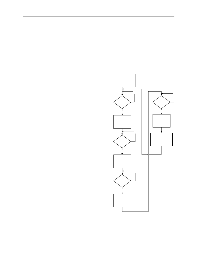
Figure 2.
Power Cycle Flow Chart
power-up
and
down
System VDD rises,
bandgap begins to function
VDD > VMIN
Read nonvolatile
store
Yes
No
Read
complete
Restore data to
user latch, drive
pins
Yes
No
Restore
complete
No
Allow user access
to latch, normal
operation
Yes
VDD < VMIN
Block new writes to
NV-Latch, user latch
Complete NV-
writes in progress
No
Yes
相關PDF資料 |
PDF描述 |
|---|---|
| FM573-S | Nonvolatile Octal Latch/Register |
| FM5820-A80U | RAC10-DA(-E)(-ST) Series - Powerline Regulated AC-DC Converters; Output Voltage (Vdc): 12V; Features: Compact AC-DC Power Supply; 10 Watt PCB Mount Package; Universal Input Voltage Range; 3000VAC Isolation; Low Output Ripple and Noise; Short Circuit Protected; UL Certified |
| FM5822-ALN | Chip Schottky Barrier Diodes - Silicon epitaxial planer type |
| FM5820-ALN | CONN HEADER .05 45X4PS GOLD SMD |
| FM5821-ALN | CONNECTOR,HEADER,20P,2X10,2MMCTR,ST,SMD |
相關代理商/技術參數 |
參數描述 |
|---|---|
| FM574-P | 制造商:未知廠家 制造商全稱:未知廠家 功能描述:Nonvolatile Octal Latch/Register |
| FM574-S | 制造商:未知廠家 制造商全稱:未知廠家 功能描述:Nonvolatile Octal Latch/Register |
| FM575 | 制造商:Black Box Corporation 功能描述:RCA A/V GOLD F/F FEEDTHR OW AV MOD GIGASTATION+ |
| FM576 | 制造商:Black Box Corporation 功能描述:RCA 3.5 MM SOLDER OW AV MOD GIGASTATION+ |
| FM580 | 制造商:RECTRON 制造商全稱:Rectron Semiconductor 功能描述:SURFACE MOUNT SCHOTTKY BARRIER RECTIFIER VOLTAGE RANGE 20 to 200 Volts CURRENT 5.0 Ampere |
發布緊急采購,3分鐘左右您將得到回復。