- 您現在的位置:買賣IC網 > PDF目錄375854 > FM93C46A (Fairchild Semiconductor Corporation) 1K-Bit Serial CMOS EEPROM(1KB的串行CMOS EEPROM) PDF資料下載
參數資料
| 型號: | FM93C46A |
| 廠商: | Fairchild Semiconductor Corporation |
| 英文描述: | 1K-Bit Serial CMOS EEPROM(1KB的串行CMOS EEPROM) |
| 中文描述: | 1K位串行CMOS EEPROM(最大的1kB的串行EEPROM中的CMOS) |
| 文件頁數: | 5/13頁 |
| 文件大小: | 120K |
| 代理商: | FM93C46A |
5
www.fairchildsemi.com
FM93C46A Rev. C.1
F
(
T
Pin Description
Chip Select (CS)
This is an active high input pin to FM93C46A EEPROM (the device)
and is generated by a master that is controlling the device. A high
level on this pin selects the device and a low level deselects the
device. All serial communications with the device is enabled only
when this pin is held high. However this pin cannot be permanently
tied high, as a rising edge on this signal is required to reset the
internal state-machine to accept a new cycle and a falling edge to
initiate an internal programming after a write cycle. All activity on the
SK, DI and DO pins are ignored while CS is held low.
Serial Clock (SK)
This is an input pin to the device and is generated by the master that
is controlling the device. This is a clock signal that synchronizes the
communication between a master and the device. All input informa-
tion (DI) to the device is latched on the rising edge of this clock input,
while output data (DO) from the device is driven from the rising edge
of this clock input. This pin is gated by CS signal.
Serial Input (DI)
This is an input pin to the device and is generated by the master
that is controlling the device. The master transfers Input informa-
tion (Start bit, Opcode bits, Array addresses and Data) serially via
this pin into the device. This Input information is latched on the
rising edge of the SCK. This pin is gated by CS signal.
Serial Output (DO)
This is an output pin from the device and is used to transfer Output
data via this pin to the controlling master. Output data is serially
shifted out on this pin from the rising edge of the SCK. This pin is
active only when the device is selected.
Organization (ORG)
This is an input pin to the device and is used to select the format
of data (16-bit or 8-bit). If this pin is tied high, 16-bit format is
selected, while if it is tied low, 8-bit format is selected. Depending
on the format selected, FM93C46A requires 6-bit address field (for
16-bit data format) or 7-bit address field (for 8-bit data format).
Refer Table 1 and Table 2 for more details. This pin is internally
pulled-up to V
CC
. Hence leaving this pin unconnected would
default to 16-bit data format.
Microwire Interface
A typical communication on the Microwire bus is made through the
CS, SK, DI and DO signals. To facilitate various operations on the
Memory array, a set of 7 instructions are implemented on
FM93C46A. The format of each instruction is listed under Table 1
(for 16-bit format) and Table 2 (for 8-bit format).
Instruction
Each of the above 7 instructions is explained under individual
instruction descriptions.
Start bit
This is a 1-bit field and is the first bit that is clocked into the device
when a Microwire cycle starts. This bit has to be
“
1
”
for a valid cycle
to begin. Any number of preceding
“
0
”
can be clocked into the
device before clocking a
“
1
”
.
Opcode
This is a 2-bit field and should immediately follow the start bit.
These two bits (along with 2 MSB of address field) select a
particular instruction to be executed.
Address Field
Depending on the selected organization, this is a 6-bit or 7-bit field
and should immediately follow the Opcode bits. In FM93C46A, all
6 bits (or 7 bits) are used for address decoding during READ,
WRITE and ERASE instructions. During all other instructions, the
MSB 2 bits are used to decode instruction (along with Opcode bits).
Data Field
Depending on the selected organization, this is a 16-bit or 8-bit
field and should immediately follow the Address bits. Only the
WRITE and WRALL instructions require this field. MSB bit (D15 or
D7) is clocked first and LSB bit (D0) is clocked last (both during
writes as well as reads).
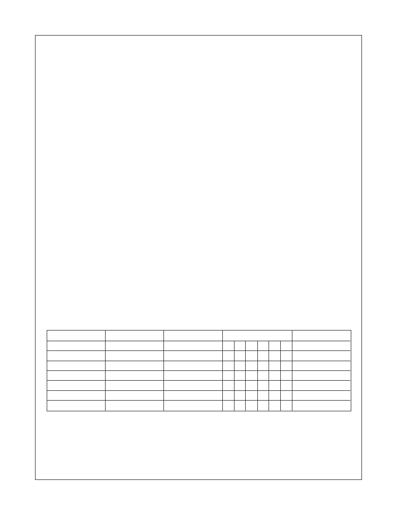
Table 1. Instruction set (16-bit organization)
Instruction
Start Bit
Opcode Field
Address Field
Data Field
READ
1
10
A5
A4
A3
A2
A1
A0
WEN
1
00
1
1
X
X
X
X
WRITE
1
01
A5
A4
A3
A2
A1
A0
D15-D0
WRALL
1
00
0
1
X
X
X
X
D15-D0
WDS
1
00
0
0
X
X
X
X
ERASE
1
11
A5
A4
A3
A2
A1
A0
ERAL
1
00
1
0
X
X
X
X
相關PDF資料 |
PDF描述 |
|---|---|
| FM93C46AE | 1K-Bit Serial CMOS EEPROM (MICROWIRE⑩ Synchronous Bus) |
| FM93C46AV | 1K-Bit Serial CMOS EEPROM (MICROWIRE⑩ Synchronous Bus) |
| FM93C46 | 1024-Bit Serial CMOS EEPROM(1024位的串行CMOS EEPROM) |
| FM93C46EM8 | Microwire Serial EEPROM |
| FM93C46EMT8 | Microwire Serial EEPROM |
相關代理商/技術參數 |
參數描述 |
|---|---|
| FM93C46AE | 制造商:FAIRCHILD 制造商全稱:Fairchild Semiconductor 功能描述:1K-Bit Serial CMOS EEPROM (MICROWIRE⑩ Synchronous Bus) |
| FM93C46AEM8 | 功能描述:電可擦除可編程只讀存儲器 USE 511-M93C46-MN6 RoHS:否 制造商:Atmel 存儲容量:2 Kbit 組織:256 B x 8 數據保留:100 yr 最大時鐘頻率:1000 KHz 最大工作電流:6 uA 工作電源電壓:1.7 V to 5.5 V 最大工作溫度:+ 85 C 安裝風格:SMD/SMT 封裝 / 箱體:SOIC-8 |
| FM93C46AEM8X | 功能描述:電可擦除可編程只讀存儲器 SOIC-8 RoHS:否 制造商:Atmel 存儲容量:2 Kbit 組織:256 B x 8 數據保留:100 yr 最大時鐘頻率:1000 KHz 最大工作電流:6 uA 工作電源電壓:1.7 V to 5.5 V 最大工作溫度:+ 85 C 安裝風格:SMD/SMT 封裝 / 箱體:SOIC-8 |
| FM93C46AEMT8 | 制造商:未知廠家 制造商全稱:未知廠家 功能描述:Microwire Serial EEPROM |
| FM93C46AEN | 功能描述:電可擦除可編程只讀存儲器 USE 511-M93C46-BN6 RoHS:否 制造商:Atmel 存儲容量:2 Kbit 組織:256 B x 8 數據保留:100 yr 最大時鐘頻率:1000 KHz 最大工作電流:6 uA 工作電源電壓:1.7 V to 5.5 V 最大工作溫度:+ 85 C 安裝風格:SMD/SMT 封裝 / 箱體:SOIC-8 |
發布緊急采購,3分鐘左右您將得到回復。