- 您現在的位置:買賣IC網 > PDF目錄375863 > FMS6366MSA28 (FAIRCHILD SEMICONDUCTOR CORP) Selectable YPbPr HD/SD 4:2:2 Video Filter Driver with Y, C and Composite Outputs PDF資料下載
參數資料
| 型號: | FMS6366MSA28 |
| 廠商: | FAIRCHILD SEMICONDUCTOR CORP |
| 元件分類: | 消費家電 |
| 英文描述: | Selectable YPbPr HD/SD 4:2:2 Video Filter Driver with Y, C and Composite Outputs |
| 中文描述: | SPECIALTY CONSUMER CIRCUIT, PDSO28 |
| 封裝: | LEAD FREE, SSOP-28 |
| 文件頁數: | 4/7頁 |
| 文件大小: | 517K |
| 代理商: | FMS6366MSA28 |
4
REV. 1B September 17, 2004
DATA SHEET
FMS6366
Applications
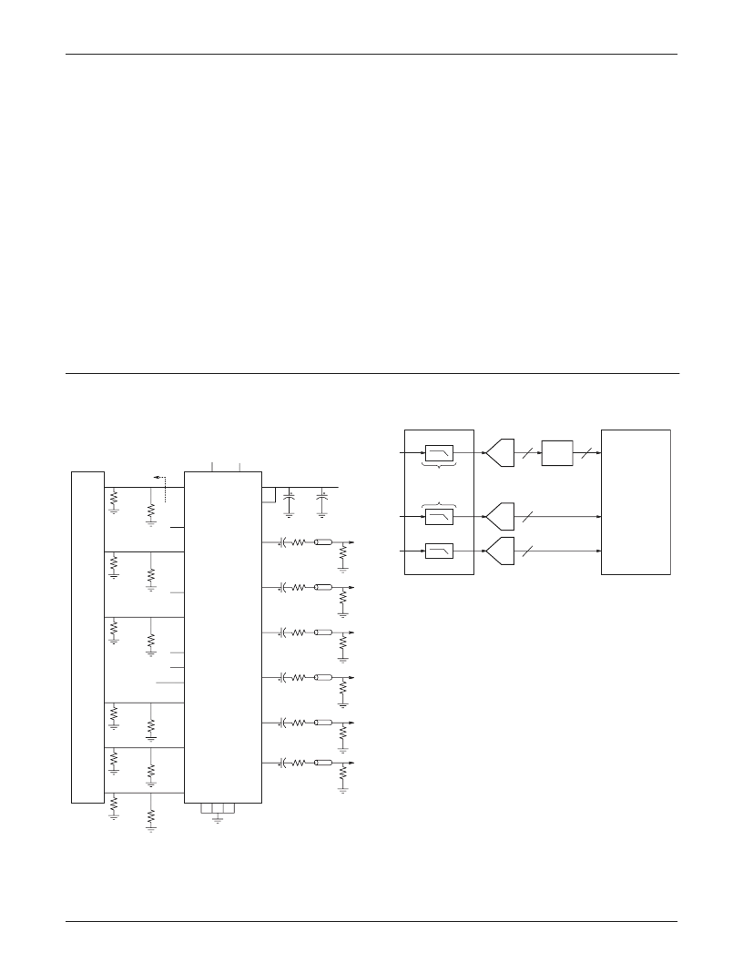
A typical application for the FMS6366 is shown in Figure 1.
Figure 1: Typical Application Diagram
Digital Delay Compensation
Figure 2: Digital Delay Compensation for
anti-alias 4:2:2 filters
The Chroma filters are one half the bandwidth of the
Luminance filter therefore the propagation delay time
through the Chroma filter is longer than the Luminance filter.
In the Standard Definition (SD) case, the Chroma filter
propagation delay is typically 60 nanoseconds longer than
the Luminance filter. This is three clock cycles at 54MHz so
it is easily corrected by adding digital delay as shown in
Figure 3 and illustrated as a shift register in Figure 2. In
the High Definition (HD) setting the Chroma filter propaga-
tion delay is typically 15 nanoseconds longer than the
Luminance filter. This is one clock cycle at 74.25MHz
so it is also easily corrected by adding digital delay to the
luminance path.
Functional Description
DC Levels
At any given time, the input signal’s DC levels must be
between 0.0V and 1.3V to utilize the optimal headroom
and to avoid clipping at the outputs. The Y channels accept
1Vpp signals with the sync tip at ground. The Pb, Pr and C
channels should be centered around 0.5V. This will ensure
that the filter will utilize the optimal headroom and avoid
clipping.
DC-Coupled Output Applications
The 220uF capacitor coupled with the 150
forms a high pass filter that blocks the DC while passing the
video frequencies and avoiding tilt. Lower values such as
10uF cause unacceptable tilt in the output signal. By AC
coupling, the average DC level is zero. Thus, the output volt-
ages of all channels will be centered around zero.
termination
DC coupling the output of the FMS6366 is allowable, but
not recommended. There are several trade-offs: The average
DC level on the outputs will be 2V. Each output will dissi-
pate an additional 40mW nominally. The application will
need to accommodate a 1V DC offset sync tip. Also, it is
recommended to limit one 150
load per output.
The FMS6366 is specified to operate with output currents
typically less than 50mA, more than sufficient for a dual
(75
) video load. Internal amplifiers are current limited to
a maximum of 100mA and should withstand brief duration
short circuit conditions, however this capability is not guar-
anteed.
Driving Digital Pins
The FMS6366 digital inputs are compatible with most
3.3V and 5V logic. Verify that the V
ih
and V
il
are within the
specified limits.
FMS6366
RSOURCE =
R
T1
|| R
T2
2
3
PbINA
PbINB
4
5
Y1INA
Y1INB
6
7
PrINA
PrINB
8
YC / N_AUX
9, 10, 15, 17
NC
12
AUXIN
14
Y2IN
13
CIN
DAC
220
μ
F
75
75
75
Video Cable
Y1OUT
23
75
75
75
Video Cable
PbOUT
22
75
75
75
Video Cable
Y2OUT
21
75
75
75
Video Cable
COUT
19
75
75
75
Video Cable
CVOUT
18
75
220
μ
F
75
75
Video Cable
PrOUT
24
VCC
VCC
26
20
220
μ
F
220
μ
F
0.1
μ
F
220
μ
F
+5V
0.1
μ
F
1
μ
F
VSS
11
16
25
27
VSSVSSVSS
16
A_NB
23
HD / N_SD
R
T2
= 75
R
T1
= 75
R
T2
= 75
R
T1
= 75
R
T2
= 75
R
T1
= 75
R
T2
= 75
R
T1
= 75
R
T2
= 75
R
T1
= 75
R
T2
= 75
R
T1
= 75
Y
A/D
Shift
Register
8-10
Pr
A/D
8-10
Pb
A/D
8-10
8-10
Video
Processing
FMS6366
Luminance
Chroma
Propagation
Delay
相關PDF資料 |
PDF描述 |
|---|---|
| FMS6366MSA28X | Selectable YPbPr HD/SD 4:2:2 Video Filter Driver with Y, C and Composite Outputs |
| FMS6400-1 | Dual Channel Video Drivers with Integrated Filters and Composite Video Summer |
| FMS6400 | Dual Channel Video Drivers with Integrated Filters and Composite Video Summer |
| FMS6400CS | Dual Channel Video Drivers with Integrated Filters and Composite Video Summer |
| FMS6400CSX | Dual Channel Video Drivers with Integrated Filters and Composite Video Summer |
相關代理商/技術參數 |
參數描述 |
|---|---|
| FMS6366MSA28X | 功能描述:視頻 IC SMG FG 5 CHANNEL RoHS:否 制造商:Fairchild Semiconductor 工作電源電壓:5 V 電源電流:80 mA 最大工作溫度:+ 85 C 封裝 / 箱體:TSSOP-28 封裝:Reel |
| FMS63671_ABA3026B WAF | 制造商:Fairchild Semiconductor Corporation 功能描述: |
| FMS63671_ABB3026B WAF | 制造商:Fairchild Semiconductor Corporation 功能描述: |
| FMS6400 | 制造商:FAIRCHILD 制造商全稱:Fairchild Semiconductor 功能描述:Dual Channel Video Drivers with Integrated Filters and Composite Video Summer |
| FMS6400-1 | 制造商:FAIRCHILD 制造商全稱:Fairchild Semiconductor 功能描述:PCB Layout Considerations for Video Filter / Drivers |
發布緊急采購,3分鐘左右您將得到回復。