- 您現在的位置:買賣IC網 > PDF目錄375932 > FSDL0365RNB (FAIRCHILD SEMICONDUCTOR CORP) Green Mode Fairchild Power Switch (FPS) PDF資料下載
參數資料
| 型號: | FSDL0365RNB |
| 廠商: | FAIRCHILD SEMICONDUCTOR CORP |
| 元件分類: | 穩壓器 |
| 英文描述: | Green Mode Fairchild Power Switch (FPS) |
| 中文描述: | 12 A SWITCHING REGULATOR, 55 kHz SWITCHING FREQ-MAX, PDIP8 |
| 封裝: | MS-001BA, DIP-8 |
| 文件頁數: | 9/20頁 |
| 文件大小: | 905K |
| 代理商: | FSDL0365RNB |
FSDL0365RNB, FSDM0365RNB
9
Functional Description
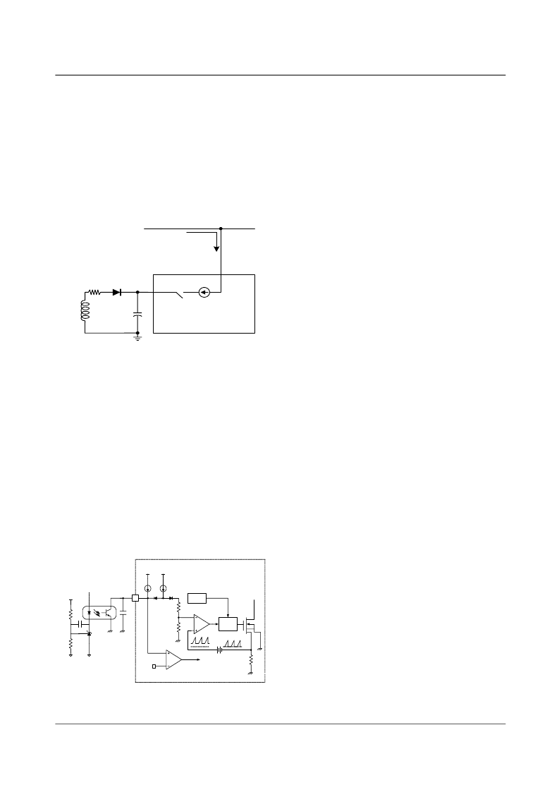
1. Startup
: In previous generations of Fairchild Power
Switches (FPS
TM
) the Vstr pin had an external resistor to the
DC input voltage line. In this generation the startup resistor
is replaced by an internal high voltage current source and a
switch that shuts off when 15ms goes by after the supply
voltage, Vcc, gets above 12V. The source turns back on if
Vcc drops below 8V.
Figure 4. High Voltage Current Source
2. Feedback Control
: The FSDx0365RNB employs current
mode control, as shown in Figure 5. An opto-coupler (such
as the H11A817A) and shunt regulator (such as the KA431)
are typically used to implement the feedback network. Com-
paring the feedback voltage with the voltage across the
Rsense resistor plus an offset voltage makes it possible to
control the switching duty cycle. When the KA431 reference
pin voltage exceeds the internal reference voltage of 2.5V,
the optocoupler LED current increases, the feedback voltage
Vfb is pulled down and it reduces the duty cycle. This event
typically happens when the input voltage is increased or the
output load is decreased.
Figure 5. Pulse Width Modulation (PWM) Circuit
3. Leading Edge Blanking (LEB)
: At the instant the inter-
nal Sense FET is turned on, the primary side capacitance and
secondary side rectifier diode reverse recovery typically
cause a high current spike through the Sense FET. Excessive
voltage across the Rsense resistor leads to incorrect feedback
operation in the current mode PWM control. To counter this
effect, the FPS employs a leading edge blanking (LEB) cir-
cuit. This circuit inhibits the PWM comparator for a short
time (t
LEB
) after the Sense FET is turned on.
4. Protection Circuits
: The FPS has several protective
functions such as over load protection (OLP), over voltage
protection (OVP), under voltage lock out (UVLO) and ther-
mal shutdown (TSD). Because these protection circuits are
fully integrated inside the IC without external components,
the reliability is improved without increasing cost. Once a
fault condition occurs, switching is terminated and the Sense
FET remains off. This causes Vcc to fall. When Vcc reaches
the UVLO stop voltage V
STOP
(8V), the protection is reset
and the internal high voltage current source charges the Vcc
capacitor via the Vstr pin. When Vcc reaches the UVLO
start voltage V
START
(12V), the FPS resumes its normal
operation. In this manner, the auto-restart can alternately
enable and disable the switching of the power Sense FET
until the fault condition is eliminated.
4.1 Over Load Protection (OLP)
:
Overload is defined as
the load current exceeding a pre-set level due to an unex-
pected event. In this situation, the protection circuit should
be activated in order to protect the SMPS. However, even
when the SMPS is operating normally, the over load protec-
tion (OLP) circuit can be activated during the load transition.
In order to avoid this undesired operation, the OLP circuit is
designed to be activated after a specified time to determine
whether it is a transient situation or an overload situation. In
conjunction with the Ipk current limit pin (if used) the cur-
rent mode feedback path would limit the current in the Sense
FET when the maximum PWM duty cycle is attained. If the
output consumes more than this maximum power, the output
voltage (Vo) decreases below its rating voltage. This reduces
the current through the opto-coupler LED, which also
reduces the opto-coupler transistor current, thus increasing
the feedback voltage (V
FB
). If V
FB
exceeds 3V, the feed-
back input diode is blocked and the 5uA current source (I
DE-
LAY
) starts to charge Cfb slowly up to Vcc. In this condition,
V
FB
increases until it reaches 6V, when the switching opera-
tion is terminated as shown in Figure 6. The shutdown delay
time is the time required to charge Cfb from 3V to 6V with
5uA current source.
Vin,dc
Vstr
Vcc
15ms after
Vcc
≥
12V
UVLO off
Vcc<8V
UVLO on
I
STR
J-FET
I
CH
3
OSC
Vcc
Vcc
5uA
0.9mA
V
SD
R
2.5R
Gate
driver
OLP
D1
D2
V
FB
Vfb
431
C
FB
Vo
+
-
V
FB,in
相關PDF資料 |
PDF描述 |
|---|---|
| FSDM0365RNB | Green Mode Fairchild Power Switch (FPS) |
| FSDM0365RL | Green Mode Fairchild Power Switch (FPSTM) |
| FSDM0365RN | Green Mode Fairchild Power Switch (FPSTM) |
| FSDL0365 | Green Mode Fairchild Power Switch (FPSTM) |
| FSDL0365RL | Green Mode Fairchild Power Switch (FPSTM) |
相關代理商/技術參數 |
參數描述 |
|---|---|
| FSDL321 | 功能描述:電源開關 IC - 配電 FPS for DVDP/STB RoHS:否 制造商:Exar 輸出端數量:1 開啟電阻(最大值):85 mOhms 開啟時間(最大值):400 us 關閉時間(最大值):20 us 工作電源電壓:3.2 V to 6.5 V 電源電流(最大值): 最大工作溫度:+ 85 C 安裝風格:SMD/SMT 封裝 / 箱體:SOT-23-5 |
| FSDL321L | 功能描述:電源開關 IC - 配電 FPS for DVDP/STB RoHS:否 制造商:Exar 輸出端數量:1 開啟電阻(最大值):85 mOhms 開啟時間(最大值):400 us 關閉時間(最大值):20 us 工作電源電壓:3.2 V to 6.5 V 電源電流(最大值): 最大工作溫度:+ 85 C 安裝風格:SMD/SMT 封裝 / 箱體:SOT-23-5 |
| FSDL321L_Q | 功能描述:電源開關 IC - 配電 FPS for DVDP/STB RoHS:否 制造商:Exar 輸出端數量:1 開啟電阻(最大值):85 mOhms 開啟時間(最大值):400 us 關閉時間(最大值):20 us 工作電源電壓:3.2 V to 6.5 V 電源電流(最大值): 最大工作溫度:+ 85 C 安裝風格:SMD/SMT 封裝 / 箱體:SOT-23-5 |
| FSDLC01G-S | 制造商:AXIOMTEK 制造商全稱:AXIOMTEK 功能描述:Capacity: 128MB to 32GB |
| FSDLC128-S | 制造商:AXIOMTEK 制造商全稱:AXIOMTEK 功能描述:Capacity: 128MB to 32GB |
發布緊急采購,3分鐘左右您將得到回復。