- 您現在的位置:買賣IC網 > PDF目錄375947 > FSYC055R (Intersil Corporation) Radiation Hardened, SEGR Resistant N-Channel Power MOSFETs PDF資料下載
參數資料
| 型號: | FSYC055R |
| 廠商: | Intersil Corporation |
| 英文描述: | Radiation Hardened, SEGR Resistant N-Channel Power MOSFETs |
| 中文描述: | 抗輻射,抗SEGR N溝道功率MOSFET |
| 文件頁數: | 2/8頁 |
| 文件大小: | 49K |
| 代理商: | FSYC055R |
2
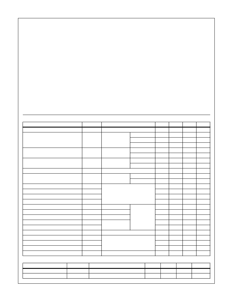
Absolute Maximum Ratings
T
C
= 25
o
C, Unless Otherwise Specified
FSYC055D, FSYC055R
60
60
UNITS
V
V
Drain to Source Voltage . . . . . . . . . . . . . . . . . . . . . . . . . . . . . . . . . . . . . . . . . . . . . . . . . . V
DS
Drain to Gate Voltage (R
GS
= 20k
) . . . . . . . . . . . . . . . . . . . . . . . . . . . . . . . . . . . . . . .V
DGR
Continuous Drain Current
T
C
= 25
o
C. . . . . . . . . . . . . . . . . . . . . . . . . . . . . . . . . . . . . . . . . . . . . . . . . . . . . . . . . . . . .I
D
T
C
= 100
o
C. . . . . . . . . . . . . . . . . . . . . . . . . . . . . . . . . . . . . . . . . . . . . . . . . . . . . . . . . . . .I
D
Pulsed Drain Current . . . . . . . . . . . . . . . . . . . . . . . . . . . . . . . . . . . . . . . . . . . . . . . . . . . . I
DM
Gate to Source Voltage . . . . . . . . . . . . . . . . . . . . . . . . . . . . . . . . . . . . . . . . . . . . . . . . . .V
GS
Maximum Power Dissipation
T
C
= 25
o
C. . . . . . . . . . . . . . . . . . . . . . . . . . . . . . . . . . . . . . . . . . . . . . . . . . . . . . . . . . . . P
T
T
C
= 100
o
C. . . . . . . . . . . . . . . . . . . . . . . . . . . . . . . . . . . . . . . . . . . . . . . . . . . . . . . . . . . P
T
Derated Above 25
o
C. . . . . . . . . . . . . . . . . . . . . . . . . . . . . . . . . . . . . . . . . . . . . . . . . . . . . .
Single Pulsed Avalanche Current, L = 100
μ
H, (See Test Figure). . . . . . . . . . . . . . . . . . . .I
AS
Continuous Source Current (Body Diode) . . . . . . . . . . . . . . . . . . . . . . . . . . . . . . . . . . . . . .I
S
Pulsed Source Current (Body Diode). . . . . . . . . . . . . . . . . . . . . . . . . . . . . . . . . . . . . . . . I
SM
Operating and Storage Temperature . . . . . . . . . . . . . . . . . . . . . . . . . . . . . . . . . . . . T
J
, T
STG
Lead Temperature (During Soldering) . . . . . . . . . . . . . . . . . . . . . . . . . . . . . . . . . . . . . . . . T
L
(Distance >0.063in (1.6mm) from Case, 10s Max)
CAUTION: Stresses above those listed in “Absolute Maximum Ratings” may cause permanent damage to the device. This is a stress only rating and operation
of the device at these or any other conditions above those indicated in the operational sections of this specification is not implied.
70 (Note)
56
200
±
20
A
A
A
V
162
65
1.30
200
70
200
W
W
W/
o
C
A
A
A
o
C
o
C
-55 to 150
300
NOTE: Current limited by package capability.
Electrical Specifications
T
C
= 25
o
C, Unless Otherwise Specified
PARAMETER
SYMBOL
TEST CONDITIONS
MIN
TYP
MAX
UNITS
Drain to Source Breakdown Voltage
BV
DSS
V
GS(TH)
I
D
= 1mA, V
GS
= 0V
V
GS
= V
DS
,
I
D
= 1mA
60
-
-
V
Gate Threshold Voltage
T
C
= -55
o
C
T
C
= 25
o
C
T
C
= 125
o
C
T
C
= 25
o
C
T
C
= 125
o
C
T
C
= 25
o
C
T
C
= 125
o
C
-
-
5.0
V
1.5
-
4.0
V
0.5
-
-
V
μ
A
μ
A
nA
Zero Gate Voltage Drain Current
I
DSS
V
DS
= 48V,
V
GS
= 0V
-
-
25
-
-
250
Gate to Source Leakage Current
I
GSS
V
GS
=
±
20V
-
-
100
-
-
200
nA
Drain to Source On-State Voltage
V
DS(ON)
r
DS(ON)12
V
GS
= 12V, I
D
= 70A
I
D
= 56A,
V
GS
= 12V
-
-
0.882
V
ns
Drain to Source On Resistance
T
C
= 25
o
C
T
C
= 125
o
C
-
0.008
0.012
-
-
0.019
Turn-On Delay Time
t
d(ON)
t
r
t
d(OFF)
t
f
Q
g(TOT)
Q
g(12)
Q
g(TH)
Q
gs
Q
gd
V
(PLATEAU)
C
ISS
C
OSS
C
RSS
R
θ
JC
V
DD
= 30V, I
D
= 70A,
R
L
= 0.43
, V
GS
= 12V,
R
GS
= 2.35
-
-
50
Rise Time
-
-
65
ns
Turn-Off Delay Time
-
-
80
ns
Fall Time
-
-
40
ns
Total Gate Charge
V
GS
= 0V to 20V
V
GS
= 0V to 12V
V
GS
= 0V to 2V
V
DD
= 30V,
I
D
= 70A
-
-
290
nC
Gate Charge at 12V
-
150
170
nC
Threshold Gate Charge
-
-
15
nC
Gate Charge Source
-
40
55
nC
Gate Charge Drain
-
53
75
nC
Plateau Voltage
I
D
= 70A, V
DS
= 15V
V
DS
= 25V, V
GS
= 0V,
f = 1MHz
-
7
-
V
Input Capacitance
-
4750
-
pF
Output Capacitance
-
2200
-
pF
Reverse Transfer Capacitance
-
475
-
pF
Thermal Resistance Junction to Case
-
-
0.77
o
C/W
Source to Drain Diode Specifications
PARAMETER
SYMBOL
TEST CONDITIONS
MIN
TYP
MAX
UNITS
Forward Voltage
V
SD
t
rr
I
SD
= 70A
I
SD
= 70A, dI
SD
/dt = 100A/
μ
s
0.6
-
1.8
V
Reverse Recovery Time
-
-
300
ns
FSYC055D, FSYC055R
相關PDF資料 |
PDF描述 |
|---|---|
| FSYC055R1 | Radiation Hardened, SEGR Resistant N-Channel Power MOSFETs |
| FSYC055R3 | Radiation Hardened, SEGR Resistant N-Channel Power MOSFETs |
| FSYC055R4 | Radiation Hardened, SEGR Resistant N-Channel Power MOSFETs |
| FSYC160D | Radiation Hardened, SEGR Resistant, N-Channel Power MOSFETs |
| FSYC160D1 | Radiation Hardened, SEGR Resistant, N-Channel Power MOSFETs |
相關代理商/技術參數 |
參數描述 |
|---|---|
| FSYC055R1 | 制造商:INTERSIL 制造商全稱:Intersil Corporation 功能描述:Radiation Hardened, SEGR Resistant N-Channel Power MOSFETs |
| FSYC055R3 | 制造商:INTERSIL 制造商全稱:Intersil Corporation 功能描述:Radiation Hardened, SEGR Resistant N-Channel Power MOSFETs |
| FSYC055R4 | 制造商:INTERSIL 制造商全稱:Intersil Corporation 功能描述:Radiation Hardened, SEGR Resistant N-Channel Power MOSFETs |
| FSYC160D | 制造商:INTERSIL 制造商全稱:Intersil Corporation 功能描述:Radiation Hardened, SEGR Resistant, N-Channel Power MOSFETs |
| FSYC160D1 | 制造商:INTERSIL 制造商全稱:Intersil Corporation 功能描述:Radiation Hardened, SEGR Resistant, N-Channel Power MOSFETs |
發布緊急采購,3分鐘左右您將得到回復。