- 您現在的位置:買賣IC網 > PDF目錄375948 > FSYE913A0R4 (INTERSIL CORP) Radiation Hardened, SEGR Resistant P-Channel Power MOSFETs PDF資料下載
參數資料
| 型號: | FSYE913A0R4 |
| 廠商: | INTERSIL CORP |
| 元件分類: | JFETs |
| 英文描述: | Radiation Hardened, SEGR Resistant P-Channel Power MOSFETs |
| 中文描述: | 9 A, 100 V, 0.28 ohm, P-CHANNEL, Si, POWER, MOSFET |
| 封裝: | CERAMIC, LCC-3 |
| 文件頁數: | 2/9頁 |
| 文件大小: | 73K |
| 代理商: | FSYE913A0R4 |
2
Absolute Maximum Ratings
T
C
= 25
o
C, Unless Otherwise Specified
FSYE913A0D, FSYE913A0R
-100
-100
UNITS
V
V
Drain to Source Voltage. . . . . . . . . . . . . . . . . . . . . . . . . . . . . . . . . . . . . . . . . . . . . . . . . . . . . V
DS
Drain to Gate Voltage (R
GS
= 20k
). . . . . . . . . . . . . . . . . . . . . . . . . . . . . . . . . . . . . . . . . .V
DGR
Continuous Drain Current
T
C
= 25
o
C . . . . . . . . . . . . . . . . . . . . . . . . . . . . . . . . . . . . . . . . . . . . . . . . . . . . . . . . . . . . . . .I
D
T
C
= 100
o
C . . . . . . . . . . . . . . . . . . . . . . . . . . . . . . . . . . . . . . . . . . . . . . . . . . . . . . . . . . . . . .I
D
Pulsed Drain Current. . . . . . . . . . . . . . . . . . . . . . . . . . . . . . . . . . . . . . . . . . . . . . . . . . . . . . . I
DM
Gate to Source Voltage . . . . . . . . . . . . . . . . . . . . . . . . . . . . . . . . . . . . . . . . . . . . . . . . . . . . . V
GS
Maximum Power Dissipation
T
C
= 25
o
C . . . . . . . . . . . . . . . . . . . . . . . . . . . . . . . . . . . . . . . . . . . . . . . . . . . . . . . . . . . . . . P
T
T
C
= 100
o
C . . . . . . . . . . . . . . . . . . . . . . . . . . . . . . . . . . . . . . . . . . . . . . . . . . . . . . . . . . . . . P
T
Linear Derating Factor . . . . . . . . . . . . . . . . . . . . . . . . . . . . . . . . . . . . . . . . . . . . . . . . . . . . . . .
Single Pulsed Avalanche Current, L = 100
μ
H, (See Test Figure) . . . . . . . . . . . . . . . . . . . . . .I
AS
Continuous Source Current (Body Diode). . . . . . . . . . . . . . . . . . . . . . . . . . . . . . . . . . . . . . . . .I
S
Pulsed Source Current (Body Diode) . . . . . . . . . . . . . . . . . . . . . . . . . . . . . . . . . . . . . . . . . . I
SM
Operating and Storage Temperature . . . . . . . . . . . . . . . . . . . . . . . . . . . . . . . . . . . . . . . T
J
, T
STG
Lead Temperature (During Soldering) . . . . . . . . . . . . . . . . . . . . . . . . . . . . . . . . . . . . . . . . . . . T
L
(Distance >0.063in (1.6mm) from Case, 10s Max)
9
5
A
A
A
V
27
±
20
42
17
0.33
27
9
27
W
W
W/
o
C
A
A
A
o
C
o
C
-55 to 150
300
CAUTION: Stresses above those listed in “Absolute Maximum Ratings” may cause permanent damage to the device. This is a stress only rating and operation of the
device at these or any other conditions above those indicated in the operational sections of this specification is not implied.
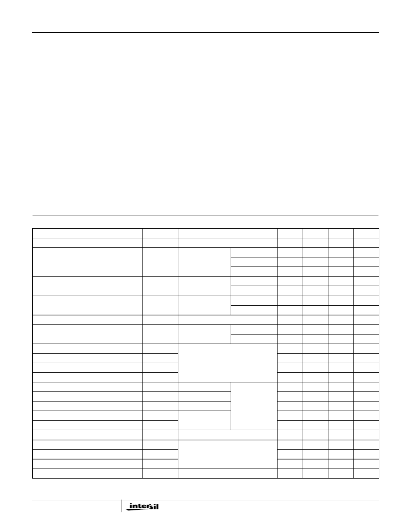
Electrical Specifications
T
C
= 25
o
C, Unless Otherwise Specified
PARAMETER
SYMBOL
TEST CONDITIONS
MIN
TYP
MAX
UNITS
Drain to Source Breakdown Voltage
BV
DSS
V
GS(TH)
I
D
= 1mA, V
GS
= 0V
V
GS
= V
DS
,
I
D
= 1mA
-100
-
-
V
Gate Threshold Voltage
T
C
= -55
o
C
T
C
= 25
o
C
T
C
= 125
o
C
T
C
= 25
o
C
T
C
= 125
o
C
T
C
= 25
o
C
T
C
= 125
o
C
-
-
-7.0
V
-2.0
-
-6.0
V
-1.0
-
-
V
Zero Gate Voltage Drain Current
I
DSS
V
DS
= -80V,
V
GS
= 0V
-
-
25
μ
A
μ
A
-
-
250
Gate to Source Leakage Current
I
GSS
V
GS
=
±
20V
-
-
100
nA
200
nA
Drain to Source On-State Voltage
V
DS(ON)
r
DS(ON)12
V
GS
= -12V, I
D
= 9A
I
D
= 5A,
V
GS
= -12V
-3.02
V
Drain to Source On Resistance
T
C
= 25
o
C
T
C
= 125
o
C
-
0.190
0.280
-
-
0.440
Turn-On Delay Time
t
d(ON)
t
r
t
d(OFF)
t
f
Q
g(TOT)
Q
g(12)
Q
g(TH)
Q
gs
Q
gd
V
(PLATEAU)
C
ISS
C
OSS
C
RSS
R
θ
JC
V
DD
= -50V, I
D
= 9A,
R
L
= 5.6
, V
GS
= -12V,
R
GS
= 7.5
-
-
20
ns
Rise Time
-
-
40
ns
Turn-Off Delay Time
-
-
40
ns
Fall Time
-
-
35
ns
Total Gate Charge
V
GS
= 0V to -20V
V
GS
= 0V to -12V
V
GS
= 0V to -2V
V
DD
= -50V,
I
D
= 9A
-
-
61
nC
Gate Charge at 12V
-
36
41
nC
Threshold Gate Charge
-
-
2.4
nC
Gate Charge Source
-
6.6
7.8
nC
Gate Charge Drain
-
17
20
nC
Plateau Voltage
I
D
= 9A, V
DS
= -15V
V
DS
= -25V, V
GS
= 0V,
f = 1MHz
-
-7
-
V
Input Capacitance
-
945
-
pF
Output Capacitance
-
315
-
pF
Reverse Transfer Capacitance
-
100
-
pF
Thermal Resistance Junction to Case
-
-
3.0
o
C/W
FSYE913A0D, FSYE913A0R
相關PDF資料 |
PDF描述 |
|---|---|
| FSYE923A0D | Radiation Hardened, SEGR Resistant P-Channel Power MOSFETs |
| FSYE923A0D1 | Radiation Hardened, SEGR Resistant P-Channel Power MOSFETs |
| FSYE923A0D3 | Radiation Hardened, SEGR Resistant P-Channel Power MOSFETs |
| FSYE923A0R | Radiation Hardened, SEGR Resistant P-Channel Power MOSFETs |
| FSYE923A0R1 | Radiation Hardened, SEGR Resistant P-Channel Power MOSFETs |
相關代理商/技術參數 |
參數描述 |
|---|---|
| FSYE923A0D | 制造商:INTERSIL 制造商全稱:Intersil Corporation 功能描述:Radiation Hardened, SEGR Resistant P-Channel Power MOSFETs |
| FSYE923A0D1 | 制造商:INTERSIL 制造商全稱:Intersil Corporation 功能描述:Radiation Hardened, SEGR Resistant P-Channel Power MOSFETs |
| FSYE923A0D3 | 制造商:INTERSIL 制造商全稱:Intersil Corporation 功能描述:Radiation Hardened, SEGR Resistant P-Channel Power MOSFETs |
| FSYE923A0R | 制造商:INTERSIL 制造商全稱:Intersil Corporation 功能描述:Radiation Hardened, SEGR Resistant P-Channel Power MOSFETs |
| FSYE923A0R1 | 制造商:INTERSIL 制造商全稱:Intersil Corporation 功能描述:Radiation Hardened, SEGR Resistant P-Channel Power MOSFETs |
發布緊急采購,3分鐘左右您將得到回復。