- 您現(xiàn)在的位置:買賣IC網(wǎng) > PDF目錄375996 > GC3011-CQ PDF資料下載
參數(shù)資料
| 型號(hào): | GC3011-CQ |
| 文件頁(yè)數(shù): | 1/34頁(yè) |
| 文件大小: | 194K |
| 代理商: | GC3011-CQ |
當(dāng)前第1頁(yè)第2頁(yè)第3頁(yè)第4頁(yè)第5頁(yè)第6頁(yè)第7頁(yè)第8頁(yè)第9頁(yè)第10頁(yè)第11頁(yè)第12頁(yè)第13頁(yè)第14頁(yè)第15頁(yè)第16頁(yè)第17頁(yè)第18頁(yè)第19頁(yè)第20頁(yè)第21頁(yè)第22頁(yè)第23頁(yè)第24頁(yè)第25頁(yè)第26頁(yè)第27頁(yè)第28頁(yè)第29頁(yè)第30頁(yè)第31頁(yè)第32頁(yè)第33頁(yè)第34頁(yè)
- 1 -
JULY 22, 1996
SLWS130
This document contains information which may be changed at any time without notice
GC3011 DIGITAL RESAMPLER
1.1
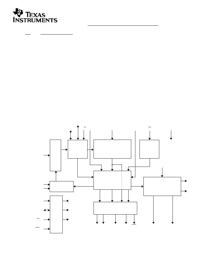
BLOCK DIAGRAM
A block diagram illustrating the major functions of the chip is shown in Figure 1
CV,FOZ,FIZ
Figure 1. GC3011 Block Diagram
DOUT[0:11]
12 bits
12 bits
INTERPOLATION FILTER
15 TAPS
4096 STEPS
16 SAMPLE
FIFO
I
C
CLK IN
OUTPUT CLOCK
GENERATOR
(FIXED CLOCK MODE OR
PLL AND VCO)
CLK
OUT
OCK
IN
OUT
FE
CKOUT
BYPASS
DATA
ERROR
INTERPOLATION
RATIO
DIN[0:11]
INTERPOLATION
MODES
OUTPUT MUX AND FORMAT
C
A[0:3]
C[0:8]
R/W
CS
TO ALL CIRCUITS
OUTPUT
MODES
OUTPUT
MODES
INTERPOLATION
RATIO
AND MODES
ERROR
ERROR
INTERPOLATION
RLL
MULTI-CHIP
SYNC
AND OFFSET
DC[0:11]
M/S
12 bits
DVAL
4 bits
8 bits
CK
SI
SYNC
CIRCUIT
HF
FRST
CK2X
SO
SI
SO
RESET
CVOUT
CVIN
EIN
EVAL
1.0
KEY FEATURES
80 million samples per second (MSPS) input rate
Fractional rate change down to 1/4
Synchronization logic to allow multi-chip complex
data operation.
Multiple chips can be synchronized with fixed delay
offsets.
Two chips allow rate changes up or down.
12 bit data I/O
32 bit rate control accumulator
16 sample output FIFO
15 tap linear phase interpolator
4096 interpolation steps
80% input passband (0 to 0.4F
th
the input rate
CK
)
+/- 0.1 dB passband ripple
Less than +/- 0.02 degrees rms phase jitter
-73 dB image rejection
60 dB worst case NPR
Adaptive rate change to lock the resampling
ratio to the output clock rate
PLL/VCO to generate an output clock to
match the rate change
Microprocessor interface for control, output,
and diagnostics
Built in diagnostics
2W power at 50 MHz, 5 volts
520 mW at 30 MHz, 3.3 volts
100 pin QFP package
相關(guān)PDF資料 |
PDF描述 |
|---|---|
| GC509 | GC509 - Class A Amplifier with 3 Independent Gain Blocks |
| GC509MCRO | Analog IC |
| GC509MINI | Analog IC |
| GC509PLID | Analog IC |
| GC509SLT | Analog IC |
相關(guān)代理商/技術(shù)參數(shù) |
參數(shù)描述 |
|---|---|
| GC3011-PQ | 制造商:Rochester Electronics LLC 功能描述:- Bulk |
| GC3021 | 制造商:TI 制造商全稱:Texas Instruments 功能描述:MIXER AND CARRIER REMOVAL CHIP |
| GC3021A | 制造商:TI 制造商全稱:Texas Instruments 功能描述:3.3V MIXER AND CARRIER REMOVAL CHIP |
| GC3021A-PQ | 功能描述:調(diào)節(jié)器/解調(diào)器 Mixer/Carrier Remover RoHS:否 制造商:Texas Instruments 封裝 / 箱體:PVQFN-N24 封裝:Reel |
| GC3021-PQ | 制造商:Rochester Electronics LLC 功能描述:- Bulk |
發(fā)布緊急采購(gòu),3分鐘左右您將得到回復(fù)。