- 您現(xiàn)在的位置:買賣IC網(wǎng) > PDF目錄370342 > GM72V66841ELT 8Mx8|3.3V|4K|75|SDR SDRAM - 64M PDF資料下載
參數(shù)資料
| 型號(hào): | GM72V66841ELT |
| 英文描述: | 8Mx8|3.3V|4K|75|SDR SDRAM - 64M |
| 中文描述: | 8Mx8 | 3.3 | 4K的| 75 | SDRAM的特別提款權(quán)- 64米 |
| 文件頁(yè)數(shù): | 1/10頁(yè) |
| 文件大小: | 81K |
| 代理商: | GM72V66841ELT |
GM72V66441ET/ELT
4,194,304 W O R D x 4 B I T x 4 B A N K
S Y N C H R O N O U S D Y N A M I C R A M
Description
T h e G M 7 2 V 6 6 4 4 1 E T / E L T i s a s y n c h r o n o u s
dynamic random access memory comprised of
67,108,864 memory cells and logic including
input and output circuits operating synchronously
by referring to the positive edge of the externally
provided Clock.
The GM72V66441ET/ELT provides four banks
o f 4 , 1 9 4 , 3 0 4 w o r d b y 4 b i t t o r e a l i z e h i g h
bandwidth with the Clock frequency up to 143
M h z .
Features
* PC133/PC100/PC66 Compatible
-7(143MHz)/-75(133MHz)/-8(125MHz)
-7K(PC100,2-2-2)/-7J(PC100,3-2-2)
* 3.3V single Power supply
* LVTTL interface
* Max Clock frequency
143/133/125/100MHz
* 4,096 refresh cycle per 64 ms
* Two kinds of refresh operation
Auto refresh / Self refresh
* Programmable burst access capability ;
- Sequence:Sequential / Interleave
- Length :1/2/4/8/FP
* Programmable CAS latency : 2/3
* 4 Banks can operate independently or
simultaneously
* Burst read/burst write or burst read/single
write operation capability
* Input and output masking by DQM input
* One Clock of back to back read or write
command interval
* Synchronous Power down and Clock
suspend capability with one Clock latency
for both entry and exit
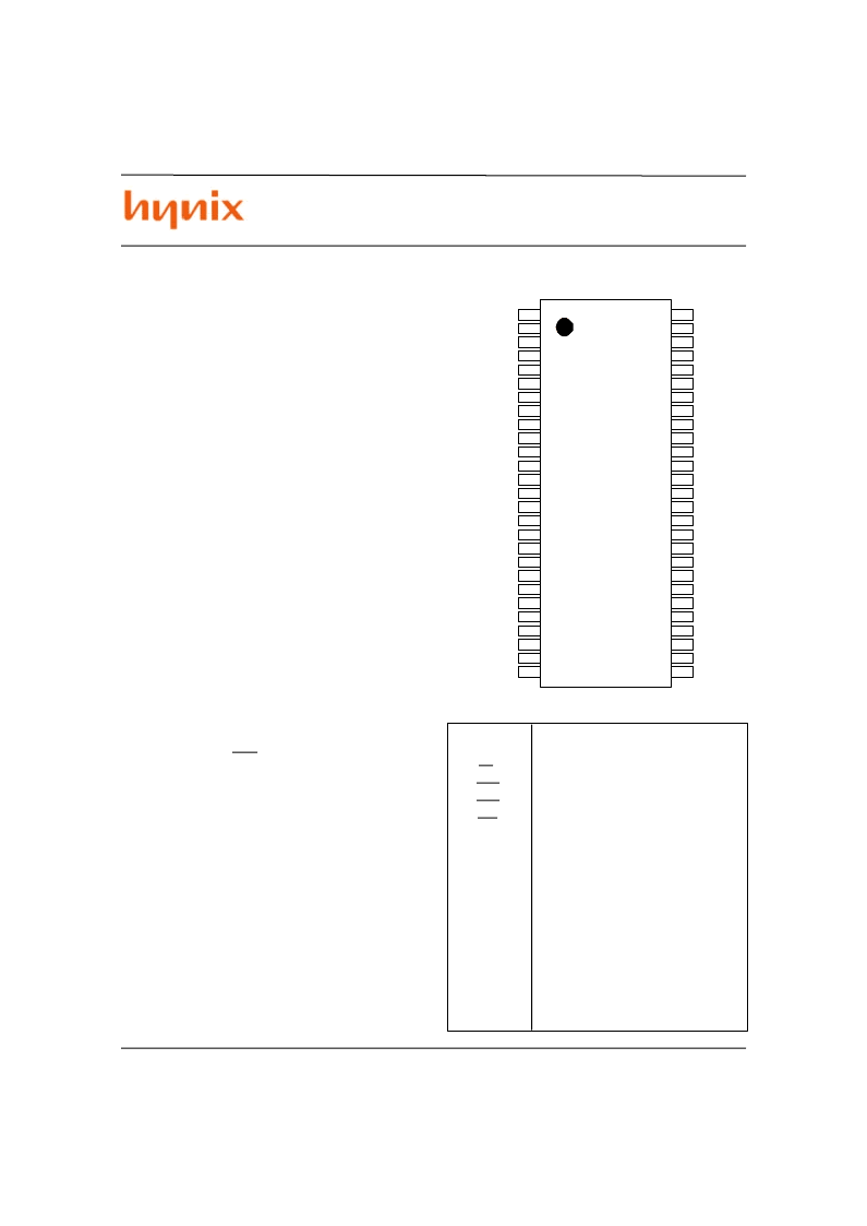
* JEDEC Standard 54Pin 400mil TSOP II Package
Pin Configuration
Pin Name
C L K
C K E
C S
R A S
C A S
W E
A0~A9,A11
A 1 0 / A P
BA0/A13
~BA1/A12
D Q 0 ~ D Q 7
D Q M
V C C Q
VSSQ
V C C
VSS
N C
Clock
Clock Enable
Chip Select
Row Address Strobe
Column Address Strobe
Write Enable
Address input
Address input or Auto Precharge
Bank select
Data input / Data output
Data input / output Mask
V
CC
for DQ
V
SS
for DQ
Power for internal circuit
Ground for internal circuit
No Connection
1
2
3
4
5
6
7
8
9
10
11
12
13
14
15
16
17
18
19
20
21
22
23
24
25
26
27
JEDEC STANDARD
400 mil 54 PIN TSOP II
(TOP VIEW)
54
53
52
51
50
49
48
47
46
45
44
43
42
41
40
39
38
37
36
35
34
33
32
31
30
29
28
V C C
N C
V C C Q
N C
D Q 0
V S S Q
N C
N C
V C C Q
N C
D Q 1
V S S Q
N C
V C C
N C
/W E
/C A S
/R A S
/C S
BA0/A13
BA1/A12
A10,AP
A 0
A 1
A 2
A 3
V C C
VSS
N C
V S S Q
N C
D Q 3
V C C Q
N C
N C
V S S Q
N C
D Q 2
V C C Q
N C
VSS
N C
D Q M
C L K
C K E
N C
A 1 1
A 9
A 8
A 7
A 6
A 5
A 4
VSS
This document is a general product description and is subject to change without notice. Hynix semiconductor does not assume any
responsibility for use of circuits described. No patent licenses are implied.
Rev. 1.1/Apr.01
相關(guān)PDF資料 |
PDF描述 |
|---|---|
| GM72V66841ET-75 | x8 SDRAM |
| GM72V66841ET-7J | x8 SDRAM |
| GM72V66841ET-8 | x8 SDRAM |
| GM76C256BL-55 | x8 SRAM |
| GM76C8128CLT-70 | x8 SRAM |
相關(guān)代理商/技術(shù)參數(shù) |
參數(shù)描述 |
|---|---|
| GM72V66841ELT-10K | 制造商:HYNIX 制造商全稱:Hynix Semiconductor 功能描述:2,097,152 WORD x 8 BIT x 4 BANK SYNCHRONOUS DYNAMIC RAM |
| GM72V66841ELT-7 | 制造商:HYNIX 制造商全稱:Hynix Semiconductor 功能描述:2,097,152 WORD x 8 BIT x 4 BANK SYNCHRONOUS DYNAMIC RAM |
| GM72V66841ELT-75 | 制造商:HYNIX 制造商全稱:Hynix Semiconductor 功能描述:2,097,152 WORD x 8 BIT x 4 BANK SYNCHRONOUS DYNAMIC RAM |
| GM72V66841ELT-7J | 制造商:HYNIX 制造商全稱:Hynix Semiconductor 功能描述:2,097,152 WORD x 8 BIT x 4 BANK SYNCHRONOUS DYNAMIC RAM |
| GM72V66841ELT-7K | 制造商:HYNIX 制造商全稱:Hynix Semiconductor 功能描述:2,097,152 WORD x 8 BIT x 4 BANK SYNCHRONOUS DYNAMIC RAM |
發(fā)布緊急采購(gòu),3分鐘左右您將得到回復(fù)。