- 您現(xiàn)在的位置:買賣IC網(wǎng) > PDF目錄385315 > GS816236D-133 (GSI TECHNOLOGY) 1M x 18, 512K x 36, 256K x 72 18Mb Sync Burst SRAMs PDF資料下載
參數(shù)資料
| 型號(hào): | GS816236D-133 |
| 廠商: | GSI TECHNOLOGY |
| 元件分類: | DRAM |
| 英文描述: | 1M x 18, 512K x 36, 256K x 72 18Mb Sync Burst SRAMs |
| 中文描述: | 512K X 36 CACHE SRAM, 8.5 ns, PBGA165 |
| 封裝: | 13 X 15 MM, 1 MM PITCH, FBGA-165 |
| 文件頁數(shù): | 26/41頁 |
| 文件大小: | 980K |
| 代理商: | GS816236D-133 |
第1頁第2頁第3頁第4頁第5頁第6頁第7頁第8頁第9頁第10頁第11頁第12頁第13頁第14頁第15頁第16頁第17頁第18頁第19頁第20頁第21頁第22頁第23頁第24頁第25頁當(dāng)前第26頁第27頁第28頁第29頁第30頁第31頁第32頁第33頁第34頁第35頁第36頁第37頁第38頁第39頁第40頁第41頁
Tex8adx6prsi hsseiiainaeNtRcmmne o NwDsg.
GS816218(B/D)/GS816236(B/D)/GS816272(C)
Specifications cited are subject to change without notice. For latest documentation see http://www.gsitechnology.com.
Rev: 2.17 11/2004
26/41
1999, GSI Technology
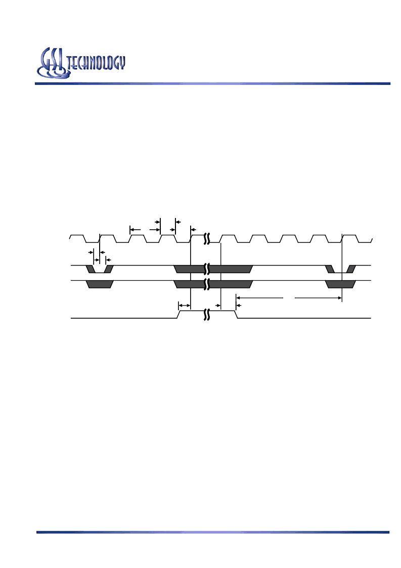
Sleep Mode
During normal operation, ZZ must be pulled low, either by the user or by its internal pull down resistor. When ZZ is pulled high,
the SRAM will enter a Power Sleep mode after 2 cycles. At this time, internal state of the SRAM is preserved. When ZZ returns to
low, the SRAM operates normally after ZZ recovery time.
Sleep mode is a low current, power-down mode in which the device is deselected and current is reduced to I
SB
2. The duration of
Sleep mode is dictated by the length of time the ZZ is in a High state. After entering Sleep mode, all inputs except ZZ become
disabled and all outputs go to High-Z The ZZ pin is an asynchronous, active high input that causes the device to enter Sleep mode.
When the ZZ pin is driven high, I
SB
2 is guaranteed after the time tZZI is met. Because ZZ is an asynchronous input, pending
operations or operations in progress may not be properly completed if ZZ is asserted. Therefore, Sleep mode must not be initiated
until valid pending operations are completed. Similarly, when exiting Sleep mode during tZZR, only a Deselect or Read commands
may be applied while the SRAM is recovering from Sleep mode.
Sleep Mode Timing Diagram
Application Tips
Single and Dual Cycle Deselect
SCD devices (like this one) force the use of “dummy read cycles” (read cycles that are launched normally, but that are ended with
the output drivers inactive) in a fully synchronous environment. Dummy read cycles waste performance, but their use usually
assures there will be no bus contention in transitions from reads to writes or between banks of RAMs. DCD SRAMs do not waste
bandwidth on dummy cycles and are logically simpler to manage in a multiple bank application (wait states need not be inserted at
bank address boundary crossings), but greater care must be exercised to avoid excessive bus contention.
tZZR
tZZH
tZZS
Hold
Setup
tKL
tKL
tKH
tKH
tKC
tKC
CK
ADSP
ADSC
ZZ
相關(guān)PDF資料 |
PDF描述 |
|---|---|
| GS816236D-133I | 1M x 18, 512K x 36, 256K x 72 18Mb Sync Burst SRAMs |
| GS816236D-150 | 1M x 18, 512K x 36, 256K x 72 18Mb Sync Burst SRAMs |
| GS816236D-150I | 1M x 18, 512K x 36, 256K x 72 18Mb Sync Burst SRAMs |
| GS816236D-166 | 1M x 18, 512K x 36, 256K x 72 18Mb Sync Burst SRAMs |
| GS816236D-166I | 1M x 18, 512K x 36, 256K x 72 18Mb Sync Burst SRAMs |
相關(guān)代理商/技術(shù)參數(shù) |
參數(shù)描述 |
|---|---|
| GS816236D-133I | 制造商:GSI Technology 功能描述:512K X 36 CACHE SRAM, 8.5 ns, PBGA165 |
| GS816236D-166I | 制造商:GSI Technology 功能描述:512K X 36 CACHE SRAM, 7 ns, PBGA165 |
| GS816236DB-150 | 制造商:GSI Technology 功能描述:119 BGA - Bulk |
| GS816236DB-150V | 制造商:GSI Technology 功能描述:119 BGA - Bulk |
| GS816236DB-200 | 制造商:GSI Technology 功能描述:119 BGA - Bulk |
發(fā)布緊急采購,3分鐘左右您將得到回復(fù)。