- 您現在的位置:買賣IC網 > PDF目錄385317 > GS8170LW72C-200I (Electronic Theatre Controls, Inc.) Low-Noise Operational Amplifier 8-SOIC -40 to 85 PDF資料下載
參數資料
| 型號: | GS8170LW72C-200I |
| 廠商: | Electronic Theatre Controls, Inc. |
| 英文描述: | Low-Noise Operational Amplifier 8-SOIC -40 to 85 |
| 中文描述: | 35.7西格馬1x1Lp的CMOS的I / O后寫入SigmaRAM |
| 文件頁數: | 1/27頁 |
| 文件大?。?/td> | 884K |
| 代理商: | GS8170LW72C-200I |
當前第1頁第2頁第3頁第4頁第5頁第6頁第7頁第8頁第9頁第10頁第11頁第12頁第13頁第14頁第15頁第16頁第17頁第18頁第19頁第20頁第21頁第22頁第23頁第24頁第25頁第26頁第27頁
GS8170LW36/72C-333/300/250/200
18Mb
Σ
1x1Lp CMOS I/O
Late Write SigmaRAM
200 MHz–333 MHz
1.8 V V
DD
1.8 V I/O
209-Bump BGA
Commercial Temp
Industrial Temp
Rev: 2.03 1/2005
Specifications cited are subject to change without notice. For latest documentation see http://www.gsitechnology.com.
1/27
2002, GSI Technology, Inc.
Features
Late Write mode, Pipelined Read mode
JEDEC-standard SigmaRAM
pinout and package
1.8 V +150/–100 mV core power supply
1.8 V CMOS Interface
ZQ controlled user-selectable output drive strength
Dual Cycle Deselect
Burst Read and Write option
Fully coherent read and write pipelines
Echo Clock outputs track data output drivers
Byte write operation (9-bit bytes)
2 user-programmable chip enable inputs
IEEE 1149.1 JTAG-compliant Serial Boundary Scan
209-bump, 14 mm x 22 mm, 1 mm bump pitch BGA package
Pin-compatible with future 36Mb, 72Mb, and 144Mb
devices
SigmaRAM Family Overview
GS8170LW36/72 SigmaRAMs are built in compliance with
the SigmaRAM pinout standard for synchronous SRAMs.
They are 18,874,368-bit (18Mb) SRAMs. This family of wide,
very low voltage CMOS I/O SRAMs is designed to operate at
the speeds needed to implement economical high performance
networking systems.
Σ
RAMs are offered in a number of configurations including
Late Write, Double Late Write, and Double Data Rate (DDR).
The logical differences between the protocols employed by
these RAMs mainly involve various approaches to write
cueing and data transfer rates. The
Σ
RAM
family standard
allows a user to implement the interface protocol best suited to
the task at hand.
Functional Description
Because SigmaRAMs are synchronous devices, address data
inputs and read/write control inputs are captured on the rising
edge of the input clock. Write cycles are internally self-timed
and initiated by the rising edge of the clock input. This feature
eliminates complex off-chip write pulse generation required by
asynchronous SRAMs and simplifies input signal timing.
Σ
RAMs support pipelined reads utilizing a rising-edge-
triggered output register. They also utilize a Dual Cycle
Deselect (DCD) output deselect protocol.
Σ
RAMs are implemented with high performance CMOS
technology and are packaged in a 209-bump BGA.
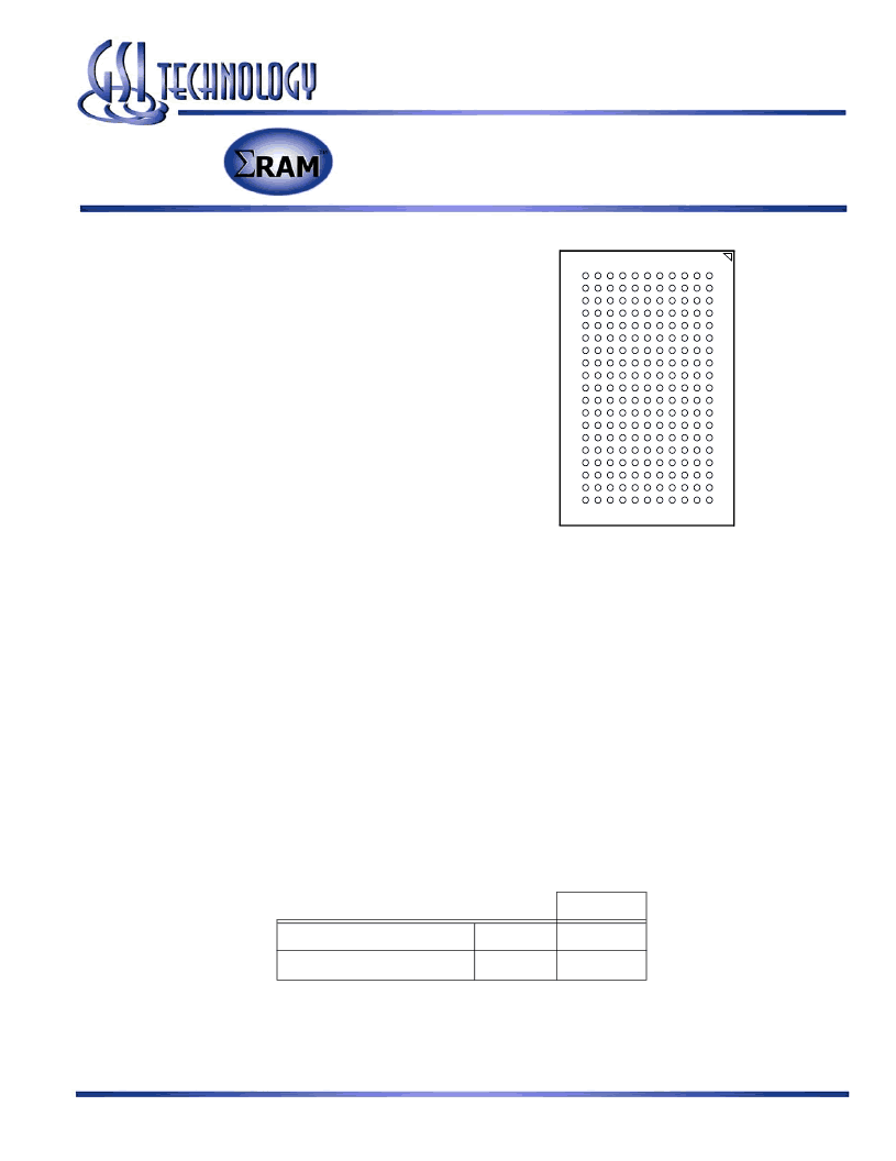
209-Bump, 14 mm x 22 mm BGA
1 mm Bump Pitch, 11 x 19 Bump Array
Bottom View
Parameter Synopsis
Key Fast Bin Specs
Symbol
- 333
Cycle Time
tKHKH
3.0 ns
Access Time
tKHQV
1.6 ns
相關PDF資料 |
PDF描述 |
|---|---|
| GS8170LW72C-250 | Low-Noise Operational Amplifier 8-SOIC -40 to 85 |
| GS8170LW72C-250I | Low-Noise Operational Amplifier 8-SOIC -40 to 85 |
| GS8170LW72C-300 | Low-Noise Operational Amplifier 8-SOIC -40 to 85 |
| GS8170LW72C-300I | Low-Noise Operational Amplifier 8-SOIC -40 to 85 |
| GS8170LW72C-333 | Low-Noise Operational Amplifier 8-PDIP -40 to 85 |
相關代理商/技術參數 |
參數描述 |
|---|---|
| GS8171DW36AC-300I | 制造商:GSI Technology 功能描述:SRAM SYNC QUAD 1.8V 18MBIT 512KX36 1.8NS 209FBGA - Trays |
| GS8171DW36AC-350 | 制造商:GSI Technology 功能描述:SRAM SYNC QUAD 1.8V 18MBIT 512KX36 1.7NS 209FBGA - Trays |
| GS8171DW36AC-350I | 制造商:GSI Technology 功能描述:SRAM SYNC QUAD 1.8V 18MBIT 512KX36 1.7NS 209BGA - Trays |
| GS8171DW36AGC-250 | 制造商:GSI Technology 功能描述:SRAM SYNC QUAD 1.8V 18MBIT 512KX36 2.1NS 209FBGA - Trays |
| GS8171DW36AGC-300 | 制造商:GSI Technology 功能描述:SRAM SYNC QUAD 1.8V 18MBIT 512KX36 1.8NS 209FBGA - Trays |
發布緊急采購,3分鐘左右您將得到回復。