- 您現在的位置:買賣IC網 > PDF目錄385328 > GS864272GC-167IV (GSI TECHNOLOGY) 4M x 18, 2M x 36, 1M x 72 72Mb S/DCD Sync Burst SRAMs PDF資料下載
參數資料
| 型號: | GS864272GC-167IV |
| 廠商: | GSI TECHNOLOGY |
| 元件分類: | DRAM |
| 英文描述: | 4M x 18, 2M x 36, 1M x 72 72Mb S/DCD Sync Burst SRAMs |
| 中文描述: | 1M X 72 CACHE SRAM, 8 ns, PBGA209 |
| 封裝: | 14 X 22 MM, 1 MM PITCH, ROHS COMPLIANT, BGA-209 |
| 文件頁數: | 26/35頁 |
| 文件大小: | 934K |
| 代理商: | GS864272GC-167IV |
第1頁第2頁第3頁第4頁第5頁第6頁第7頁第8頁第9頁第10頁第11頁第12頁第13頁第14頁第15頁第16頁第17頁第18頁第19頁第20頁第21頁第22頁第23頁第24頁第25頁當前第26頁第27頁第28頁第29頁第30頁第31頁第32頁第33頁第34頁第35頁
Preliminary
GS864218/36/72(B/C)-xxxV
Specifications cited are subject to change without notice. For latest documentation see http://www.gsitechnology.com.
Rev: 1.03 6/2006
26/35
2004, GSI Technology
Tap Controller Instruction Set
Overview
There are two classes of instructions defined in the Standard 1149.1-1990; the standard (Public) instructions, and device specific
(Private) instructions. Some Public instructions are mandatory for 1149.1 compliance. Optional Public instructions must be
implemented in prescribed ways. The TAP on this device may be used to monitor all input and I/O pads, and can be used to load
address, data or control signals into the RAM or to preload the I/O buffers.
When the TAP controller is placed in Capture-IR state the two least significant bits of the instruction register are loaded with 01.
When the controller is moved to the Shift-IR state the Instruction Register is placed between TDI and TDO. In this state the desired
instruction is serially loaded through the TDI input (while the previous contents are shifted out at TDO). For all instructions, the
TAP executes newly loaded instructions only when the controller is moved to Update-IR state. The TAP instruction set for this
device is listed in the following table.
Select DR
Capture DR
0
Shift DR
Exit1 DR
Pause DR
Exit2 DR
Update DR
1
Select IR
Capture IR
0
Shift IR
Exit1 IR
Pause IR
Exit2 IR
Update IR
1
Test Logic Reset
Run Test Idle
0
1
0
1
1
0
1
1
1
0
0
1
1
0
0
0
0
1
1
0
0
0
0
0
1
1
1
1
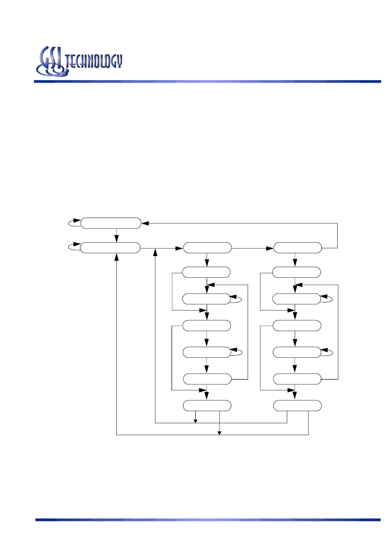
JTAG Tap Controller State Diagram
Instruction Descriptions
BYPASS
When the BYPASS instruction is loaded in the Instruction Register the Bypass Register is placed between TDI and TDO. This
occurs when the TAP controller is moved to the Shift-DR state. This allows the board level scan path to be shortened to facili-
tate testing of other devices in the scan path.
相關PDF資料 |
PDF描述 |
|---|---|
| GS864272GC-167V | 4M x 18, 2M x 36, 1M x 72 72Mb S/DCD Sync Burst SRAMs |
| GS864272GC-200IV | 4M x 18, 2M x 36, 1M x 72 72Mb S/DCD Sync Burst SRAMs |
| GS864272GC-200V | 4M x 18, 2M x 36, 1M x 72 72Mb S/DCD Sync Burst SRAMs |
| GS864272GC-250IV | 4M x 18, 2M x 36, 1M x 72 72Mb S/DCD Sync Burst SRAMs |
| GS864272GC-250V | 4M x 18, 2M x 36, 1M x 72 72Mb S/DCD Sync Burst SRAMs |
相關代理商/技術參數 |
參數描述 |
|---|---|
| GS864272GC-167V | 制造商:GSI Technology 功能描述:SRAM SYNC DUAL 1.8V/2.5V 72MBIT 1MX72 8NS/3.4NS 209BGA - Bulk |
| GS864272GC-200 | 制造商:GSI Technology 功能描述:SRAM SYNC OCTAL 2.5V/3.3V 72MBIT 1MX72 7.5NS/3NS 209FBGA - Trays |
| GS864272GC-200I | 制造商:GSI Technology 功能描述:SRAM SYNC OCTAL 2.5V/3.3V 72MBIT 1MX72 7.5NS/3NS 209FBGA - Trays |
| GS864272GC-200IV | 制造商:GSI Technology 功能描述:SRAM SYNC DUAL 1.8V/2.5V 72MBIT 1MX72 7.5NS/3NS 209BGA - Bulk |
| GS864272GC-200V | 制造商:GSI Technology 功能描述:SRAM SYNC DUAL 1.8V/2.5V 72MBIT 1MX72 7.5NS/3NS 209BGA - Bulk |
發布緊急采購,3分鐘左右您將得到回復。