- 您現(xiàn)在的位置:買賣IC網(wǎng) > PDF目錄385334 > GS8662D09GE-167 (GSI TECHNOLOGY) 72Mb SigmaQuad-II Burst of 4 SRAM PDF資料下載
參數(shù)資料
| 型號: | GS8662D09GE-167 |
| 廠商: | GSI TECHNOLOGY |
| 元件分類: | DRAM |
| 英文描述: | 72Mb SigmaQuad-II Burst of 4 SRAM |
| 中文描述: | 8M X 9 DDR SRAM, 0.5 ns, PBGA165 |
| 封裝: | 15 X 17 MM, 1 MM PITCH, ROHS COMPLIANT, FPBGA-165 |
| 文件頁數(shù): | 7/29頁 |
| 文件大小: | 896K |
| 代理商: | GS8662D09GE-167 |
第1頁第2頁第3頁第4頁第5頁第6頁當(dāng)前第7頁第8頁第9頁第10頁第11頁第12頁第13頁第14頁第15頁第16頁第17頁第18頁第19頁第20頁第21頁第22頁第23頁第24頁第25頁第26頁第27頁第28頁第29頁
Preliminary
GS8662D08/09/18/36E-333/300/250/200/167
Specifications cited are subject to change without notice. For latest documentation see http://www.gsitechnology.com.
Rev: 1.01a 2/2006
7/29
2005, GSI Technology
Background
Separate I/O SRAMs, from a system architecture point of view, are attractive in applications where alternating reads and writes are
needed. Therefore, the SigmaQuad-II SRAM interface and truth table are optimized for alternating reads and writes. Separate I/O
SRAMs are unpopular in applications where multiple reads or multiple writes are needed because burst read or write transfers from
Separate I/O SRAMs can cut the RAM’s bandwidth in half.
Alternating Read-Write Operations
SigmaQuad-II SRAMs follow a few simple rules of operation.
- Read or Write commands issued on one port are never allowed to interrupt an operation in progress on the other port.
- Read or Write data transfers in progress may not be interrupted and re-started.
- R and W high always deselects the RAM.
- All address, data, and control inputs are sampled on clock edges.
In order to enforce these rules, each RAM combines present state information with command inputs. See the Truth Table for
details.
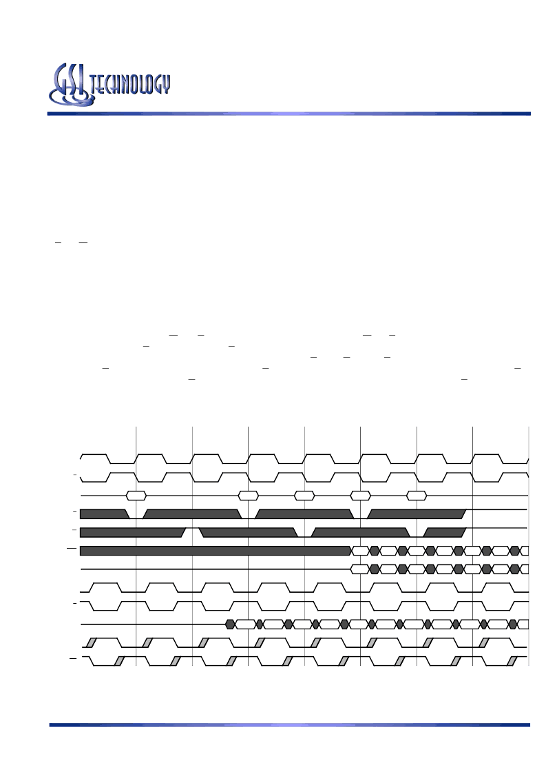
SigmaQuad-II B4 SRAM DDR Read
The status of the Address Input, W, and R pins are sampled by the rising edges of K. W and R high causes chip disable. A low on
the Read Enable-bar pin, R, begins a read cycle. R is always ignored if the previous command loaded was a read command. Data
can be clocked out after the next rising edge of K with a rising edge of C (or by K if C and C are tied high), after the following
rising edge of K with a rising edge of C (or by K if C and C are tied high), after the next rising edge of K with a rising edge of C,
and after the following rising edge of K with a rising edge of C. Clocking in a high on the Read Enable-bar pin, R, begins a read
port deselect cycle.
SigmaQuad-II B4 Double Data Rate SRAM Read First
Read A
NOP
Read B
Write C
Read D
Write E
NOP
A
B
C
D
E
C
C+1
C+2
C+3
E
E+1
C
C+1
C+2
C+3
E
E+1
A
A+1
A+2
A+3
B
B+1
B+2
B+3
D
D+1
D+2
K
K
Address
R
W
BWx
D
C
C
Q
CQ
CQ
相關(guān)PDF資料 |
PDF描述 |
|---|---|
| GS8662D09GE-167I | 72Mb SigmaQuad-II Burst of 4 SRAM |
| GS8662D09GE-200 | 72Mb SigmaQuad-II Burst of 4 SRAM |
| GS8662D09GE-200I | 72Mb SigmaQuad-II Burst of 4 SRAM |
| GS8662D09GE-250 | 72Mb SigmaQuad-II Burst of 4 SRAM |
| GS8662D09GE-250I | 72Mb SigmaQuad-II Burst of 4 SRAM |
相關(guān)代理商/技術(shù)參數(shù) |
參數(shù)描述 |
|---|---|
| GS8662D09GE-167I | 制造商:GSI 制造商全稱:GSI Technology 功能描述:72Mb SigmaQuad-II Burst of 4 SRAM |
| GS8662D09GE-200 | 制造商:GSI 制造商全稱:GSI Technology 功能描述:72Mb SigmaQuad-II Burst of 4 SRAM |
| GS8662D09GE-200I | 制造商:GSI 制造商全稱:GSI Technology 功能描述:72Mb SigmaQuad-II Burst of 4 SRAM |
| GS8662D09GE-250 | 制造商:GSI 制造商全稱:GSI Technology 功能描述:72Mb SigmaQuad-II Burst of 4 SRAM |
| GS8662D09GE-250I | 制造商:GSI 制造商全稱:GSI Technology 功能描述:72Mb SigmaQuad-II Burst of 4 SRAM |
發(fā)布緊急采購,3分鐘左右您將得到回復(fù)。