- 您現(xiàn)在的位置:買賣IC網(wǎng) > PDF目錄385334 > GS8662D09GE-167I (GSI TECHNOLOGY) 72Mb SigmaQuad-II Burst of 4 SRAM PDF資料下載
參數(shù)資料
| 型號: | GS8662D09GE-167I |
| 廠商: | GSI TECHNOLOGY |
| 元件分類: | DRAM |
| 英文描述: | 72Mb SigmaQuad-II Burst of 4 SRAM |
| 中文描述: | 8M X 9 DDR SRAM, 0.5 ns, PBGA165 |
| 封裝: | 15 X 17 MM, 1 MM PITCH, ROHS COMPLIANT, FPBGA-165 |
| 文件頁數(shù): | 13/29頁 |
| 文件大小: | 896K |
| 代理商: | GS8662D09GE-167I |
第1頁第2頁第3頁第4頁第5頁第6頁第7頁第8頁第9頁第10頁第11頁第12頁當(dāng)前第13頁第14頁第15頁第16頁第17頁第18頁第19頁第20頁第21頁第22頁第23頁第24頁第25頁第26頁第27頁第28頁第29頁
Preliminary
GS8662D08/09/18/36E-333/300/250/200/167
Specifications cited are subject to change without notice. For latest documentation see http://www.gsitechnology.com.
Rev: 1.01a 2/2006
13/29
2005, GSI Technology
FLXDrive-II Output Driver Impedance Control
HSTL I/O SigmaQuad-II SRAMs are supplied with programmable impedance output drivers. The ZQ pin must be connected to
V
SS
via an external resistor, RQ, to allow the SRAM to monitor and adjust its output driver impedance. The value of RQ must be
5X the value of the desired RAM output impedance. The allowable range of RQ to guarantee impedance matching continuously is
between 150
and 300
. Periodic readjustment of the output driver impedance is necessary as the impedance is affected by drifts
in supply voltage and temperature. The SRAM’s output impedance circuitry compensates for drifts in supply voltage and
temperature. A clock cycle counter periodically triggers an impedance evaluation, resets and counts again. Each impedance
evaluation may move the output driver impedance level one step at a time towards the optimum level. The output driver is
implemented with discrete binary weighted impedance steps. Updates of pull-down drive impedance occur whenever a driver is
producing a “1” or is High-Z. Pull-up drive impedance is updated when a driver is producing a “0” or is High-Z.
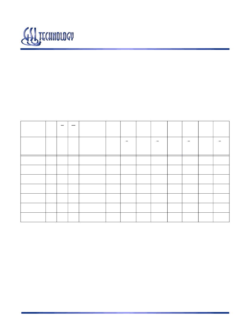
Separate I/O SigmaQuad-II B4 SRAM Truth Table
Previous
Operation
A
R
W
Current
Operation
D
D
D
D
Q
Q
Q
Q
K
↑
(t
n-1
)
K
↑
(t
n
)
K
↑
(t
n
)
K
↑
(t
n
)
K
↑
(t
n
)
K
↑
(t
n+1
)
K
↑
(t
n+1
)
K
↑
(t
n+2
)
K
↑
(t
n+2
)
K
↑
(t
n+1
)
K
↑
(t
n+1
)
K
↑
(t
n+2
)
K
↑
(t
n+2
)
Deselect
X
1
1
Deselect
X
X
—
—
Hi-Z
Hi-Z
—
—
Write
X
1
X
Deselect
D2
D3
—
—
Hi-Z
Hi-Z
—
—
Read
X
X
1
Deselect
X
X
—
—
Q2
Q3
—
—
Deselect
V
1
0
Write
D0
D1
D2
D3
Hi-Z
Hi-Z
—
—
Deselect
V
0
X
Read
X
X
—
—
Q0
Q1
Q2
Q3
Read
V
X
0
Write
D0
D1
D2
D3
Q2
Q3
—
—
Write
V
0
X
Read
D2
D3
—
—
Q0
Q1
Q2
Q3
Notes:
1.
2.
3.
4.
5.
“1” = input “high”; “0” = input “l(fā)ow”; “V” = input “valid”; “X” = input “don’t care”
“—” indicates that the input requirement or output state is determined by the next operation.
Q0, Q1, Q2, and Q3 indicate the first, second, third, and fourth pieces of output data transferred during Read operations.
D0, D1, D2, and D3 indicate the first, second, third, and fourth pieces of input data transferred during Write operations.
Qs are tristated for one cycle in response to Deselect and Write commands, one cycle after the command is sampled, except when pre-
ceded by a Read command.
Users should not clock in metastable addresses.
6.
相關(guān)PDF資料 |
PDF描述 |
|---|---|
| GS8662D09GE-200 | 72Mb SigmaQuad-II Burst of 4 SRAM |
| GS8662D09GE-200I | 72Mb SigmaQuad-II Burst of 4 SRAM |
| GS8662D09GE-250 | 72Mb SigmaQuad-II Burst of 4 SRAM |
| GS8662D09GE-250I | 72Mb SigmaQuad-II Burst of 4 SRAM |
| GS8662D09GE-300 | 72Mb SigmaQuad-II Burst of 4 SRAM |
相關(guān)代理商/技術(shù)參數(shù) |
參數(shù)描述 |
|---|---|
| GS8662D09GE-200 | 制造商:GSI 制造商全稱:GSI Technology 功能描述:72Mb SigmaQuad-II Burst of 4 SRAM |
| GS8662D09GE-200I | 制造商:GSI 制造商全稱:GSI Technology 功能描述:72Mb SigmaQuad-II Burst of 4 SRAM |
| GS8662D09GE-250 | 制造商:GSI 制造商全稱:GSI Technology 功能描述:72Mb SigmaQuad-II Burst of 4 SRAM |
| GS8662D09GE-250I | 制造商:GSI 制造商全稱:GSI Technology 功能描述:72Mb SigmaQuad-II Burst of 4 SRAM |
| GS8662D09GE-300 | 制造商:GSI 制造商全稱:GSI Technology 功能描述:72Mb SigmaQuad-II Burst of 4 SRAM |
發(fā)布緊急采購,3分鐘左右您將得到回復(fù)。