- 您現在的位置:買賣IC網 > PDF目錄385343 > GS88218BB-200I (GSI TECHNOLOGY) 512K x 18, 256K x 36 9Mb SCD/DCD Sync Burst SRAMs PDF資料下載
參數資料
| 型號: | GS88218BB-200I |
| 廠商: | GSI TECHNOLOGY |
| 元件分類: | DRAM |
| 英文描述: | 512K x 18, 256K x 36 9Mb SCD/DCD Sync Burst SRAMs |
| 中文描述: | 512K X 18 CACHE SRAM, 6.5 ns, PBGA119 |
| 封裝: | FPBGA-119 |
| 文件頁數: | 15/37頁 |
| 文件大小: | 751K |
| 代理商: | GS88218BB-200I |
第1頁第2頁第3頁第4頁第5頁第6頁第7頁第8頁第9頁第10頁第11頁第12頁第13頁第14頁當前第15頁第16頁第17頁第18頁第19頁第20頁第21頁第22頁第23頁第24頁第25頁第26頁第27頁第28頁第29頁第30頁第31頁第32頁第33頁第34頁第35頁第36頁第37頁
GS88218/36BB/D-333/300/250/200/150
Rev: 1.02 10/2004
Specifications cited are subject to change without notice. For latest documentation see http://www.gsitechnology.com.
15/37
2002, GSI Technology
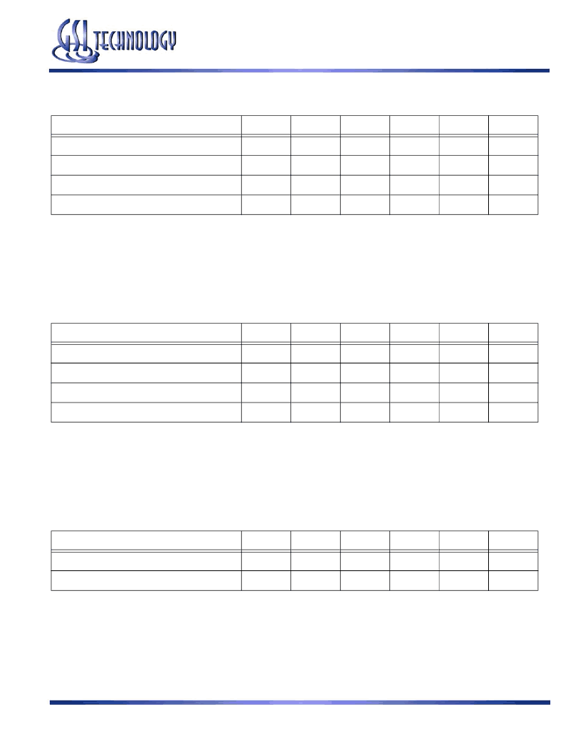
V
DDQ3
Range Logic Levels
Parameter
Symbol
Min.
Typ.
Max.
Unit
Notes
V
DD
Input High Voltage
V
IH
2.0
—
V
DD
+ 0.3
V
1
V
DD
Input Low Voltage
V
IL
–
0.3
—
0.8
V
1
V
DDQ
I/O Input High Voltage
V
IHQ
2.0
—
V
DDQ
+ 0.3
V
1,3
V
DDQ
I/O Input Low Voltage
V
ILQ
–
0.3
—
0.8
V
1,3
Notes:
1.
The part numbers of Industrial Temperature Range versions end the character “I”. Unless otherwise noted, all performance specifica-
tions quoted are evaluated for worst case in the temperature range marked on the device.
Input Under/overshoot voltage must be
–
2 V > Vi < V
DDn
+2 V not to exceed 4.6 V maximum, with a pulse width not to exceed 20% tKC.
V
IHQ
(max) is voltage on V
DDQ
pins plus 0.3 V.
2.
3.
V
DDQ2
Range Logic Levels
Parameter
Symbol
Min.
Typ.
Max.
Unit
Notes
V
DD
Input High Voltage
V
IH
0.6*V
DD
—
V
DD
+ 0.3
V
1
V
DD
Input Low Voltage
V
IL
–
0.3
—
0.3*V
DD
V
1
V
DDQ
I/O Input High Voltage
V
IHQ
0.6*V
DD
—
V
DDQ
+ 0.3
V
1,3
V
DDQ
I/O Input Low Voltage
V
ILQ
–
0.3
—
0.3*V
DD
V
1,3
Notes:
1.
The part numbers of Industrial Temperature Range versions end the character “I”. Unless otherwise noted, all performance specifica-
tions quoted are evaluated for worst case in the temperature range marked on the device.
Input Under/overshoot voltage must be
–
2 V > Vi < V
DDn
+2 V not to exceed 4.6 V maximum, with a pulse width not to exceed 20% tKC.
V
IHQ
(max) is voltage on V
DDQ
pins plus 0.3 V.
2.
3.
Recommended Operating Temperatures
Parameter
Symbol
Min.
Typ.
Max.
Unit
Notes
Ambient Temperature (Commercial Range Versions)
T
A
0
25
70
°
C
2
Ambient Temperature (Industrial Range Versions)
T
A
–
40
25
85
°
C
2
Notes:
1.
The part numbers of Industrial Temperature Range versions end the character “I”. Unless otherwise noted, all performance specifica-
tions quoted are evaluated for worst case in the temperature range marked on the device.
Input Under/overshoot voltage must be
–
2 V > Vi < V
DDn
+2 V not to exceed 4.6 V maximum, with a pulse width not to exceed 20% tKC.
2.
相關PDF資料 |
PDF描述 |
|---|---|
| GS88218BB-250 | 512K x 18, 256K x 36 9Mb SCD/DCD Sync Burst SRAMs |
| GS88218BB-250I | 512K x 18, 256K x 36 9Mb SCD/DCD Sync Burst SRAMs |
| GS88218BB-300 | 512K x 18, 256K x 36 9Mb SCD/DCD Sync Burst SRAMs |
| GS88218BB-3005I | 512K x 18, 256K x 36 9Mb SCD/DCD Sync Burst SRAMs |
| GS88218BB-333 | 512K x 18, 256K x 36 9Mb SCD/DCD Sync Burst SRAMs |
相關代理商/技術參數 |
參數描述 |
|---|---|
| GS88218CB-200 | 制造商:GSI Technology 功能描述:SRAM SYNC DUAL 2.5V/3.3V 9MBIT 512KX18 6.5NS/3NS 119FPBGA - Trays |
| GS88218CB-200I | 制造商:GSI Technology 功能描述:SRAM SYNC DUAL 2.5V/3.3V 9MBIT 512KX18 6.5NS/3NS 119FPBGA - Trays |
| GS88218CB-200IV | 制造商:GSI Technology 功能描述:SRAM SYNC DUAL 1.8V/2.5V 9MBIT 512KX18 6.5NS/3NS 119FPBGA - Trays |
| GS88218CB-200V | 制造商:GSI Technology 功能描述:SRAM SYNC DUAL 1.8V/2.5V 9MBIT 512KX18 6.5NS/3NS 119FPBGA - Trays |
| GS88218CB-250 | 制造商:GSI Technology 功能描述:SRAM SYNC DUAL 2.5V/3.3V 9MBIT 512KX18 5.5NS/2.5NS 119FPBGA - Trays |
發布緊急采購,3分鐘左右您將得到回復。