- 您現在的位置:買賣IC網 > PDF目錄383056 > GY4102ACDA (Electronic Theatre Controls, Inc.) Fast Toggling Video Switch PDF資料下載
參數資料
| 型號: | GY4102ACDA |
| 廠商: | Electronic Theatre Controls, Inc. |
| 英文描述: | Fast Toggling Video Switch |
| 中文描述: | 快速切換為視頻開關 |
| 文件頁數: | 1/5頁 |
| 文件大小: | 117K |
| 代理商: | GY4102ACDA |
Document No. 520 - 21 - 2
GENNUM CORPORATION P.O. Box 489, Stn A, Burlington, Ontario, Canada L7R 3Y3 tel. (416) 632-2996 fax: (416) 632-2055 telex: 061-8525
Japan Branch: B-210 Miyamae Village, 2-10-42 Miyamae, Suginami-ku, Tokyo 168, Japan tel. (03) 3247-8838 fax: (03) 3247-8839
CIRCUIT DESCRIPTION
The GY4102A is a bipolar, monolithic SPDT video switch
incorporating fast control logic. The analog signal path is
characterised by low differential gain, low differential phase
and low insertion loss, coupled with a
±
0.1 dB bandwidth
of typically 100 MHz into a 10 pF load, using an external
series resistor.
In demanding video applications the GY4102A features a
typical switching glitch of less than 30 mV over a 3 ns
period. The device offers toggle rates up to 50 MHz. The
control input is TTL and 5 V CMOS compatible.
APPLICATIONS
Sub-pixel video switching
Fast data sampling
Modulation
Special Effects video switching
TOP VIEW
4
5
8
PIN 1
OUT
V
EE
IN 0
IN 1
CTRL
V
CC
8 PIN PDIP
8 PIN SOIC
0 IN 0
1 IN 1
CTRL OUTPUT
PIN CONNECTIONS
TRUTH TABLE
AVAILABLE PACKAGING
8 pin PDIP
8 pin SOIC
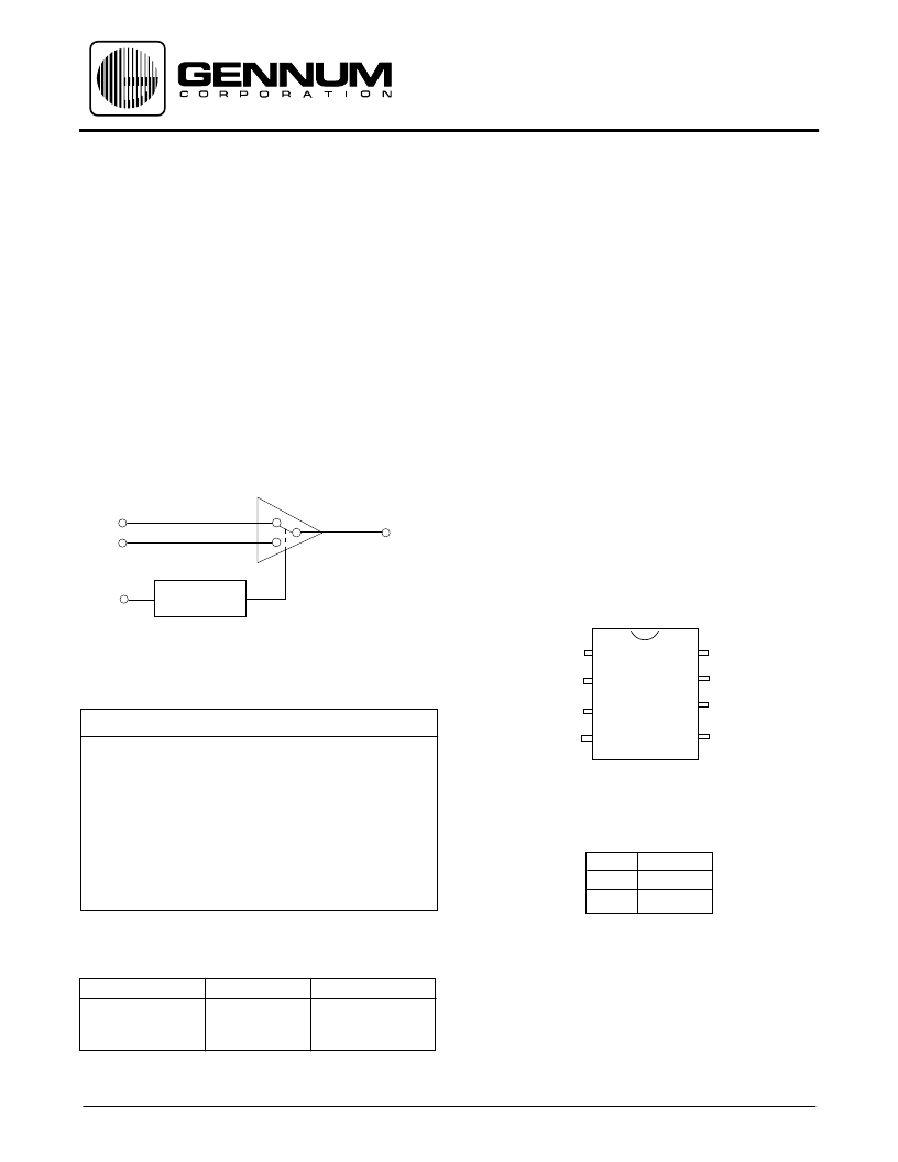
CTRL
IN 1
IN 0
CONTROL
LOGIC
OUT
GND 1
GND 2
FEATURES
FUNCTIONAL BLOCK DIAGRAM
ABSOLUTE MAXIMUM RATINGS
PARAMETER
VALUE
Supply Voltage
±
6.0 V
Operating Temperature Range
0
°
C to 70
°
C
Storage Temperature Range
-65
°
C to 150
°
C
Lead Temperature
(Soldering, 10 Sec)
260
°
C
Analog Input Voltage (
IN 0, IN 1
)
V
EE
<V
IN
<V
CC
+0.3 V
Control Input Voltage Range -5 V < V
CTRL
< V
CC
+0.3 V
ORDERING INFORMATION
Part Number Package Type Temperature Range
GY4102ACDA
8 pin PDIP
0 - 70
o
C
GY4102ACKA
8 pin SOIC
0 - 70
o
C
DATA SHEET
20 ns switching time (toggle)
make-before-break switching
100 MHz at
±
0.1dB, bandwidth (flattened)
typically 0.04 dB insertion loss at 1 MHz
typically 0.03 % differential gain at 3.58 MHz
typically 0.01 degree differential phase at 3.58 MHz
GY4102A Fast Toggling
Video Switch
相關PDF資料 |
PDF描述 |
|---|---|
| GY4102ACKA | Fast Toggling Video Switch |
| HA-2602883 | Wideband, High Impedance Operational Amplifier |
| HA-2626 | 100MHz, High Input Impedance, Very Wideband, Uncompensated Operational Amplifiers |
| HA-2705 | Low Power, High Performance Operational Amplifier |
| HA3-2705-5 | Low Power, High Performance Operational Amplifier |
相關代理商/技術參數 |
參數描述 |
|---|---|
| GY4102ACKA | 制造商:Gennum Corporation 功能描述: |
| GY4102ACKAE3 | 制造商:Semtech Corporation 功能描述:Analog Switch Single SPDT 8-Pin SOIC 制造商:Semtech Corporation 功能描述:Analog Multiplexer |
| GY50NC60WD | 制造商:STMICROELECTRONICS 制造商全稱:STMicroelectronics 功能描述:N-channel 600V - 50A - Max247 Very fast PowerMESH IGBT |
| GY7-12 | 制造商:RINO MECH.(GENGARELL 功能描述: |
| GY9.5 | 制造商:ALLIED LEDS 功能描述:LAMP HOLDER, MED BI-PIN BASE 18 AWG |
發布緊急采購,3分鐘左右您將得到回復。