- 您現在的位置:買賣IC網 > PDF目錄385353 > HA5352 (Intersil Corporation) Fast Acquisition Dual Sample and Hold Amplifier PDF資料下載
參數資料
| 型號: | HA5352 |
| 廠商: | Intersil Corporation |
| 元件分類: | 運動控制電子 |
| 英文描述: | Fast Acquisition Dual Sample and Hold Amplifier |
| 中文描述: | 快速采集雙采樣保持放大器 |
| 文件頁數: | 2/5頁 |
| 文件大小: | 133K |
| 代理商: | HA5352 |
3-2
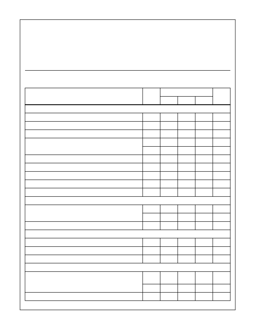
Specifications HA5352
Absolute Maximum Ratings
Operating Conditions
Voltage Between V+ and V- Terminals . . . . . . . . . . . . . . . . . . +11V
Differential Input Voltage . . . . . . . . . . . . . . . . . . . . . . . . . . . . . . +6V
Voltage between S/H control and ground. . . . . . . . . . . . . . . . .+5.5V
Output Current, Continuous
. . . . . . . . . . . . . . . . . . . . . . . . . . . . .±
37mA
Junction Temperature (Plastic Packages) . . . . . . . . . . . . . . +150
o
C
Lead Temperature (Soldering, 10s) . . . . . . . . . . . . . . . . . . . +300
o
C
(SOIC - Lead Tips Only)
Operating Temperature Range
HA5352I. . . . . . . . . . . . . . . . . . . . . . . . . . . . . -40
o
C
≤
T
A
≤
+85
o
C
Storage Temperature Range . . . . . . . . . . . . . -65
o
C
≤
T
A
≤
+150
o
C
Thermal Package Characteristics
Plastic DIP. . . . . . . . . . . . . . . . . . . . . . . . . . . . . . . . . .
SOIC . . . . . . . . . . . . . . . . . . . . . . . . . . . . . . . . . . . . . .
θ
JA
90
o
C/W
95
o
C/W
CAUTION: Stresses above those listed in “Absolute Maximum Ratings” may cause permanent damage to the device. This is a stress only rating and operation
of the device at these or any other conditions above those indicated in the operational sections of this specification is not implied.
Electrical Specifications
Test Conditions: V
SUPPLY
=
±
5V; C
H
= Internal = 15pF, Digital Input: V
IL
= +0.0V (Sample), V
IH
= 4.0V
(Hold). Non-Inverting Unity Gain Configuration (Output Tied to -Input), C
L
= 5pF, Unless Otherwise
Specified
PARAMETERS
TEMP
HA5352I
UNITS
MIN
TYP
MAX
INPUT CHARACTERISTICS
Input Voltage Range
Full
-2.5
-
+2.5
V
Input Resistance (Note 2)
+25
o
C
100
500
-
k
Input Capacitance
+25
o
C
-
-
5
pF
Input Offset Voltage
+25
o
C
-2
-
2
mV
Full
-3.0
-
3.0
mV
Offset Voltage Temperature Coefficient
Full
-
15
-
μ
V/
o
C
Bias Current
Full
-
2.5
5
μ
A
Offset Current
Full
-1.5
-
+1.5
μ
A
Common Mode Range
Full
-2.5
-
+2.5
V
Common Mode Rejection (
±
2.5V
DC
, Note 3)
Full
60
80
-
dB
TRANSFER CHARACTERISTICS
Large Signal Voltage Gain
(±
2.5V
OUT
)
+25
o
C
95
108
-
dB
Full
85
-
-
dB
Unity Gain -3dB Bandwidth
+25
o
C
-
40
-
MHz
TRANSIENT RESPONSE
Rise Time (200mV Step)
+25
o
C
-
8.5
-
ns
Overshoot (200mV Step)
+25
o
C
0
-
30
%
Slew Rate (5V Step)
Full
88
105
-
V/
μ
s
DIGITAL INPUT CHARACTERISTICS
Input Voltage (High)
V
IH
+25
o
C,
+85
o
C
2.1
-
5.0
V
-40
o
C
2.4
-
5.0
V
Input Voltage (Low)
V
IL
Full
0
-
0.8
V
相關PDF資料 |
PDF描述 |
|---|---|
| HA5352883 | Fast Acquisition Dual Sample and Hold Amplifier |
| HA5352IP | Fast Acquisition Dual Sample and Hold Amplifier |
| HA5352IB | Fast Acquisition Dual Sample and Hold Amplifier |
| HA7-5147R5254 | 120MHz, Ultra-Low Noise Precision Operational Amplifiers |
| HA7-5222883 | Dual, Low Noise, Wideband, Precision Operational Amplifier |
相關代理商/技術參數 |
參數描述 |
|---|---|
| HA5352/883 | 制造商:INTERSIL 制造商全稱:Intersil Corporation 功能描述:Fast Acquisition Dual Sample and Hold Amplifier |
| HA5352883 | 制造商:INTERSIL 制造商全稱:Intersil Corporation 功能描述:Fast Acquisition Dual Sample and Hold Amplifier |
| HA5352IB | 制造商:INTERSIL 制造商全稱:Intersil Corporation 功能描述:Fast Acquisition Dual Sample and Hold Amplifier |
| HA5352IB WAF | 制造商:Harris Corporation 功能描述: |
| HA5352IP | 制造商:INTERSIL 制造商全稱:Intersil Corporation 功能描述:Fast Acquisition Dual Sample and Hold Amplifier |
發布緊急采購,3分鐘左右您將得到回復。