- 您現在的位置:買賣IC網 > PDF目錄385375 > HFA1135IB96 (INTERSIL CORP) GT 3C 3#16S SKT RECP BOX PDF資料下載
參數資料
| 型號: | HFA1135IB96 |
| 廠商: | INTERSIL CORP |
| 元件分類: | 音頻/視頻放大 |
| 英文描述: | GT 3C 3#16S SKT RECP BOX |
| 中文描述: | 1 CHANNEL, VIDEO PREAMPLIFIER, PDSO8 |
| 封裝: | PLASTIC, MS-012AA, SOIC-8 |
| 文件頁數: | 2/15頁 |
| 文件大小: | 220K |
| 代理商: | HFA1135IB96 |
2
Absolute Maximum Ratings
T
A
= 25
o
C
Thermal Information
Voltage Between V+ and V- . . . . . . . . . . . . . . . . . . . . . . . . . . . . 11V
DC Input Voltage . . . . . . . . . . . . . . . . . . . . . . . . . . . . . . . . V
SUPPLY
Differential Input Voltage . . . . . . . . . . . . . . . . . . . . . . . . . . . . . . . 8V
Output Current (Note 1). . . . . . . . . . . . . . . . .Short Circuit Protected
30mA Continuous
60mA
≤
50% Duty Cycle
ESD Rating . . . . . . . . . . . . . . . . . . . . . . . . . . . . . . . . . . . . . . >600V
Operating Conditions
Temperature Range. . . . . . . . . . . . . . . . . . . . . . . . . . -40
o
C to 85
o
C
Thermal Resistance (Typical, Note 1)
SOIC Package . . . . . . . . . . . . . . . . . . . . . . . . . . . . .
Maximum Junction Temperature (Die Only) . . . . . . . . . . . . . . . .175
o
C
Maximum Junction Temperature (Plastic Package) . . . . . . . .150
o
C
Maximum Storage Temperature Range. . . . . . . . . . -65
o
C to 150
o
C
Maximum Lead Temperature (Soldering 10s) . . . . . . . . . . . . 300
o
C
(SOIC - Lead Tips Only)
θ
JA
(
o
C/W)
165
CAUTION: Stresses above those listed in “Absolute Maximum Ratings” may cause permanent damage to the device. This is a stress only rating and operation of the
device at these or any other conditions above those indicated in the operational sections of this specification is not implied.
NOTE:
1.
θ
JA
is measured with the component mounted on a low effective thermal conductivity test board in free air. See Tech Brief TB379 for details.
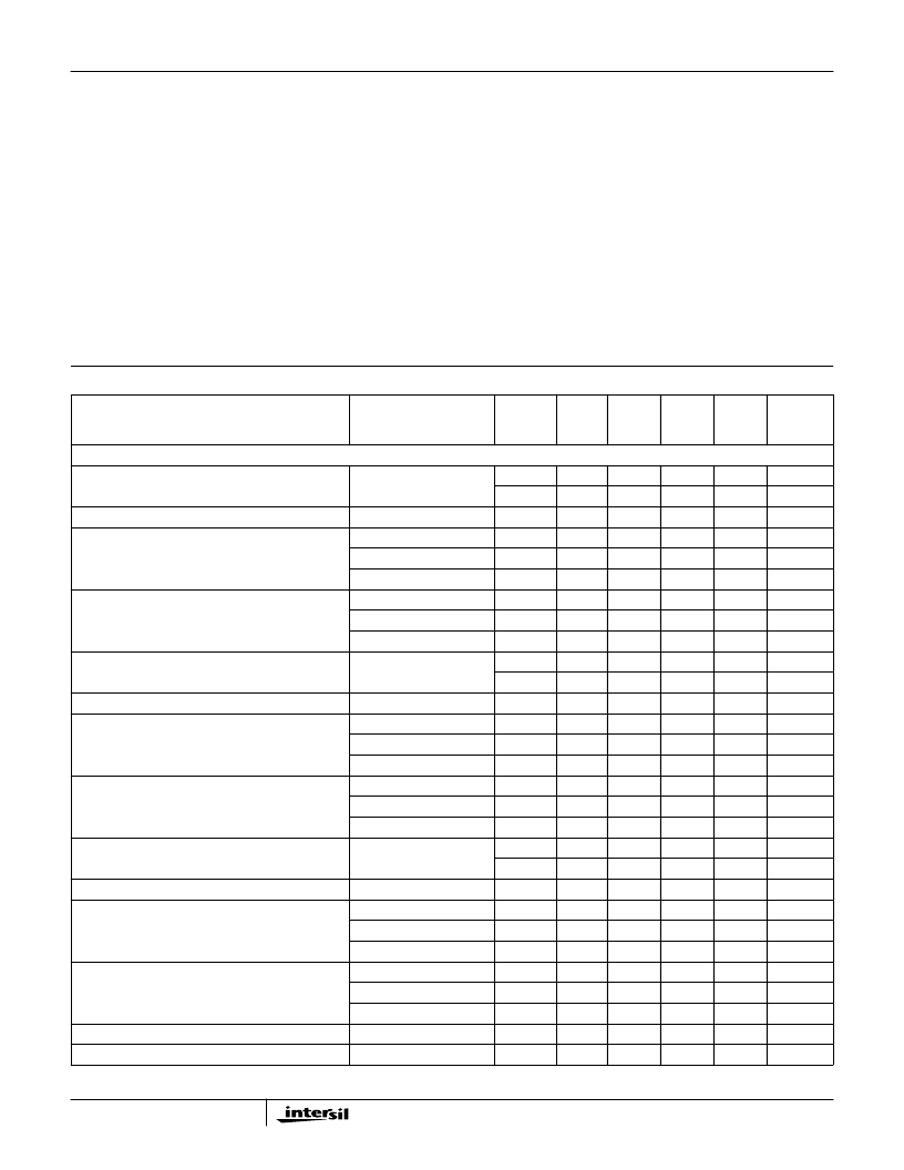
Electrical Specifications
V
SUPPLY
=
±
5V, A
V
= +1, R
F
= 510
(Note 3), R
L
= 100
,
Unless Otherwise Specified
PARAMETER
TEST CONDITIONS
(NOTE 2)
TEST
LEVEL
TEMP.
(
o
C)
MIN
TYP
MAX
UNITS
INPUT CHARACTERISTICS
Input Offset Voltage
A
25
-
2
5
mV
A
Full
-
3
8
mV
μ
V/
o
C
Average Input Offset Voltage Drift
B
Full
-
1
10
Input Offset Voltage
Common-Mode Rejection Ratio
V
CM
=
±
1.8V
V
CM
=
±
1.8V
V
CM
=
±
1.2V
V
PS
=
±
1.8V
V
PS
=
±
1.8V
V
PS
=
±
1.2V
A
25
47
50
-
dB
A
85
45
48
-
dB
A
-40
45
48
-
dB
Input Offset Voltage
Power Supply Rejection Ratio
A
25
50
54
-
dB
A
85
47
50
-
dB
A
-40
47
50
-
dB
Non-Inverting Input Bias Current
A
25
-
6
15
μ
A
μ
A
A
Full
-
10
25
Non-Inverting Input Bias Current Drift
B
Full
-
5
60
nA/
o
C
Non-Inverting Input Bias Current
Power Supply Sensitivity
V
PS
=
±
1.8V
V
PS
=
±
1.8V
V
PS
=
±
1.2V
V
CM
=
±
1.8V
V
CM
=
±
1.8V
V
CM
=
±
1.2V
A
25
-
0.5
1
μ
A/V
μ
A/V
μ
A/V
M
M
M
μ
A
μ
A
nA/
o
C
A
85
-
0.8
3
A
-40
-
0.8
3
Non-Inverting Input Resistance
A
25
0.8
2
-
A
85
0.5
1.3
-
A
-40
0.5
1.3
-
Inverting Input Bias Current
A
25
-
0.1
4
A
Full
-
3
8
Inverting Input Bias Current Drift
B
Full
-
60
200
Inverting Input Bias Current
Common-Mode Sensitivity
V
CM
=
±
1.8V
V
CM
=
±
1.8V
V
CM
=
±
1.2V
V
PS
=
±
1.8V
V
PS
=
±
1.8V
V
PS
=
±
1.2V
A
25
-
3
6
μ
A/V
μ
A/V
μ
A/V
μ
A/V
μ
A/V
μ
A/V
A
85
-
4
8
A
-40
-
4
8
Inverting Input Bias Current
Power Supply Sensitivity
A
25
-
2
5
A
85
-
4
8
A
-40
-
4
8
Inverting Input Resistance
C
25
-
40
-
Input Capacitance (Either Input)
C
25
-
1.6
-
pF
HFA1135
相關PDF資料 |
PDF描述 |
|---|---|
| HFA1135IB | 360MHz, Low Power, Video Operational Amplifier with Output Limiting |
| HFA1135EVAL | 360MHz, Low Power, Video Operational Amplifier with Output Limiting |
| HFA1135 | 360MHz, Low Power, Video Operational Amplifier with Output Limiting(360MHz、低功耗視頻運算放大器(帶輸出限制)) |
| HFA1205IP | 2.5V 144-mc CPLD - NOT RECOMMENDED for NEW DESIGN |
| HFA1205IB | Circular Connector; MIL SPEC:MIL-C-26482, Series I, Solder; Body Material:Aluminum; Series:PT06; No. of Contacts:55; Connector Shell Size:22; Connecting Termination:Solder; Circular Shell Style:Straight Plug |
相關代理商/技術參數 |
參數描述 |
|---|---|
| HFA1135IBZ | 功能描述:視頻放大器 W/ANNEAL OPAMP 360MH ZCFBLIMIT8SOICIND RoHS:否 制造商:ON Semiconductor 通道數量:4 電源類型: 工作電源電壓:3.3 V, 5 V 電源電流: 最小工作溫度: 最大工作溫度: 封裝 / 箱體:TSSOP-14 封裝:Reel |
| HFA1135IBZ | 制造商:Intersil Corporation 功能描述:IC VIDEO OP AMP 360MHZ |
| HFA1135IBZ96 | 功能描述:視頻放大器 W/ANNEAL OPAMP 360MHZ CFB LIMIT IND RoHS:否 制造商:ON Semiconductor 通道數量:4 電源類型: 工作電源電壓:3.3 V, 5 V 電源電流: 最小工作溫度: 最大工作溫度: 封裝 / 箱體:TSSOP-14 封裝:Reel |
| HFA1135MJ/883 | 制造商:Rochester Electronics LLC 功能描述:- Bulk |
| HFA1135ML/883 | 制造商:Rochester Electronics LLC 功能描述:- Bulk |
發布緊急采購,3分鐘左右您將得到回復。