- 您現(xiàn)在的位置:買賣IC網(wǎng) > PDF目錄385381 > HI5905QML (Intersil Corporation) 14 Bits 5MSPS Military A/D Converter(14位、5MSPS軍用ADC) PDF資料下載
參數(shù)資料
| 型號: | HI5905QML |
| 廠商: | Intersil Corporation |
| 英文描述: | 14 Bits 5MSPS Military A/D Converter(14位、5MSPS軍用ADC) |
| 中文描述: | 14位5MSPS軍事的A / D轉(zhuǎn)換器(14位,5MSPS軍用藝發(fā)局) |
| 文件頁數(shù): | 4/8頁 |
| 文件大小: | 93K |
| 代理商: | HI5905QML |
4-4
Detailed Description
Theory of Operation
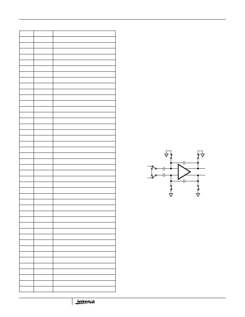
The HI5905 is a 14-bit fully differential sampling pipeline A/D
converter with digital error correction. Figure 3 depicts the
circuit for the front end differential-in-differential-out sample-
and-hold (S/H). The switches are controlled by an internal
clock which is a non-overlapping two phase signal,
φ
1
and
φ
2
, derived from the master clock. During the sampling
phase,
φ
1
, the input signal is applied to the sampling
capacitors, C
S
. At the same time the holding capacitors, C
H
,
are discharged to analog ground. At the falling edge of
φ
1
the input signal is sampled on the bottom plates of the
sampling capacitors. In the next clock phase,
φ
2
, the two
bottom plates of the sampling capacitors are connected
together and the holding capacitors are switched to the op
amp output nodes. The charge then redistributes between
C
S
and C
H
completing one sample-and-hold cycle. The
output is a fully-differential, sampled-data representation of
the analog input. The circuit not only performs the sample-
and-hold function but will also convert a single-ended input
to a fully-differential output for the converter core. During the
sampling phase, the V
IN
pins see only the on-resistance of a
switch and C
S
. The relatively small values of these
components result in a typical full power input bandwidth of
100MHz for the converter.
As illustrated in the functional block diagram and the timing
diagram in Figure 1, four identical pipeline subconverter
stages, each containing a four-bit flash converter, a four-bit
digital-to-analog converter and an amplifier with a voltage
gain of 8, follow the S/H circuit with the fifth stage being only
a 4-bit flash converter. Each converter stage in the pipeline
will be sampling in one phase and amplifying in the other
clock phase. Each individual sub-converter clock signal is
offset by 180 degrees from the previous stage clock signal,
with the result that alternate stages in the pipeline will
perform the same operation.
The output of each of the four-bit subconverter stages is a
four-bit digital word containing a supplementary bit to be
used by the digital error correction logic. The output of each
subconverter stage is input to a digital delay line which is
controlled by the internal sampling clock. The function of the
digital delay line is to time align the digital outputs of the four
Pin Descriptions
PIN #
NAME
DESCRIPTION
1
NC
No Connection
2
NC
No Connection
3
D
GND1
NC
Digital Ground
4
No Connection
5
AV
CC
A
GND
NC
Analog Supply (5.0V)
6
Analog Ground
7
No Connection
8
NC
No Connection
9
V
IN
+
V
IN
-
V
DC
NC
Positive Analog Input
10
Negative Analog Input
11
DC Bias Voltage Output
12
No Connection
13
V
ROUT
V
RIN
A
GND
AV
CC
NC
Reference Voltage Output
14
Reference Voltage Input
15
Analog Ground
16
Analog Supply (5.0V)
17
No Connection
18
D13
Data Bit 11 Output (MSB)
19
D12
Data Bit 11 Output
20
D11
Data Bit 11 Output
21
D10
Data Bit 10 Output
22
NC
No Connection
23
NC
No Connection
24
D9
Data Bit 9 Output
25
D8
Data Bit 8 Output
26
D
GND2
DV
CC2
NC
Digital Ground
27
Digital Supply (5.0V)
28
No Connection
29
D7
Data Bit 7 Output
30
D6
Data Bit 6 Output
31
D5
Data Bit 5 Output
32
D4
Data Bit 4 Output
33
D3
Data Bit 3 Output
34
NC
No Connection
35
NC
No Connection
36
D2
Data Bit 2 Output
37
D1
Data Bit 1 Output
38
D0
Data Bit 0 Output (LSB)
39
NC
No Connection
40
CLK
Input Clock
41
DV
CC1
D
GND1
DV
CC1
NC
Digital Supply (5.0V)
42
Digital Ground
43
Digital Supply (5.0V)
44
No Connection
C
H
C
S
C
S
V
IN
+
V
OUT
+
V
OUT
-
V
IN
-
φ
1
φ
1
φ
2
φ
1
φ
1
C
H
φ
1
φ
1
+
-
-
+
FIGURE 3. ANALOG INPUT SAMPLE-AND-HOLD
相關(guān)PDF資料 |
PDF描述 |
|---|---|
| HI5905 | 14-Bit, 5 MSPS A/D Converter |
| HI5905IN | 14-Bit, 5 MSPS A/D Converter |
| HI5905N | 14-Bit, 5 MSPS, Military A/D Converter |
| HI5905EVAL2 | 14-Bit, 5 MSPS A/D Converter |
| HI7106 | 3 1/2 Digit, LCD/LED Display, A/D Converter |
相關(guān)代理商/技術(shù)參數(shù) |
參數(shù)描述 |
|---|---|
| HI5960 | 制造商:INTERSIL 制造商全稱:Intersil Corporation 功能描述:14-Bit, 125+MSPS, CommLinkTM High Speed D/A Converter |
| HI5960_05 | 制造商:INTERSIL 制造商全稱:Intersil Corporation 功能描述:14-Bit, 125+MSPS, CommLinkTM High Speed D/A Converter |
| HI5960IA | 功能描述:CONV D/A 14BIT 130MSPS 28-TSSOP RoHS:否 類別:集成電路 (IC) >> 數(shù)據(jù)采集 - 數(shù)模轉(zhuǎn)換器 系列:- 標(biāo)準(zhǔn)包裝:2,400 系列:- 設(shè)置時間:- 位數(shù):18 數(shù)據(jù)接口:串行 轉(zhuǎn)換器數(shù)目:3 電壓電源:模擬和數(shù)字 功率耗散(最大):- 工作溫度:-40°C ~ 85°C 安裝類型:表面貼裝 封裝/外殼:36-TFBGA 供應(yīng)商設(shè)備封裝:36-TFBGA 包裝:帶卷 (TR) 輸出數(shù)目和類型:* 采樣率(每秒):* |
| HI5960IA-T | 功能描述:CONV D/A 14BIT 130MSPS 28-TSSOP RoHS:否 類別:集成電路 (IC) >> 數(shù)據(jù)采集 - 數(shù)模轉(zhuǎn)換器 系列:- 標(biāo)準(zhǔn)包裝:2,400 系列:- 設(shè)置時間:- 位數(shù):18 數(shù)據(jù)接口:串行 轉(zhuǎn)換器數(shù)目:3 電壓電源:模擬和數(shù)字 功率耗散(最大):- 工作溫度:-40°C ~ 85°C 安裝類型:表面貼裝 封裝/外殼:36-TFBGA 供應(yīng)商設(shè)備封裝:36-TFBGA 包裝:帶卷 (TR) 輸出數(shù)目和類型:* 采樣率(每秒):* |
| HI5960IAZ | 功能描述:數(shù)模轉(zhuǎn)換器- DAC 28 -40 85C 14 BIT 125MSPS CMOS DAC RoHS:否 制造商:Texas Instruments 轉(zhuǎn)換器數(shù)量:1 DAC 輸出端數(shù)量:1 轉(zhuǎn)換速率:2 MSPs 分辨率:16 bit 接口類型:QSPI, SPI, Serial (3-Wire, Microwire) 穩(wěn)定時間:1 us 最大工作溫度:+ 85 C 安裝風(fēng)格:SMD/SMT 封裝 / 箱體:SOIC-14 封裝:Tube |
發(fā)布緊急采購,3分鐘左右您將得到回復(fù)。