- 您現在的位置:買賣IC網 > PDF目錄385381 > HI7190EVAL (Intersil Corporation) null24-Bit, High Precision, Sigma Delta A/D Converter PDF資料下載
參數資料
| 型號: | HI7190EVAL |
| 廠商: | Intersil Corporation |
| 英文描述: | null24-Bit, High Precision, Sigma Delta A/D Converter |
| 中文描述: | null24位,精度高,Σ-ΔA / D轉換 |
| 文件頁數: | 17/24頁 |
| 文件大小: | 187K |
| 代理商: | HI7190EVAL |
1887
Write Operation
Data can be written to the Control Register, Offset Calibra-
tion Register, Positive Full Scale Calibration Register, and
the Negative Full Scale Calibration Register. Write opera-
tions are done using the SDIO, CS and SCLK lines only, as
all data is written into the HI7190 via the SDIO line even
when using the 3-wire configuration. Figures 15 and 16
show typical write timing diagrams.
The communication cycle is started by asserting the CS line
low and starting the clock from its idle state. To assert a write
cycle, during the instruction phase of the communication
cycle, the Instruction Byte should be set to a write transfer
(R/W = 1).
When writing to the serial port, data is latched into the
HI7190 on the rising edge of SCLK. Data can then be
changed on the falling edge of SCLK. Data can also be
changed on the rising edge of SCLK due to the 0ns hold
time required on the data. This is useful in pipelined applica-
tions where the data is latched on the rising edge of the
clock.
Read Operation - 3-Wire Transfer
Data can be read from the Data Output Register, Control
Register, Offset Calibration Register, Positive Full Scale
Calibration Register, and the Negative Full Scale Calibration
Register. When configured in 3-wire transfer mode, read
operations are done using the SDIO, SDO, CS and SCLK
lines. All data is read via the SDO line. Figures 17 and 18
show typical 3-wire read timing diagrams.
The communication cycle is started by asserting the CS line
and starting the clock from its idle state. To assert a read
cycle, during the instruction phase of the communication
cycle, the Instruction Byte should be set to a read transfer
(R/W = 0).
When reading the serial port, data is driven out of the
HI7190 on the falling edge of SCLK. Data can be registered
externally on the next rising edge of SCLK.
Read Operation - 2-Wire Transfer
Data can be read from the Data Output Register, Control
Register, Offset Calibration Register, Positive Full Scale Cal-
ibration Register, and the Negative Full Scale Calibration
Register. When configured in two-wire transfer mode, read
operations are done using the SDIO, CS and SCLK lines. All
data is read via the SDIO line. Figures 19 and 20 show
typical 2-wire read timing diagrams.
The communication cycle is started by asserting the CS line
and starting the clock from its idle state. To assert a read cycle,
during the instruction phase of the communication cycle, the
Instruction Byte should be set to a read transfer (R/W = 0).
When reading the serial port, data is driven out of the
HI7190 on the falling edge of SCLK. Data can be registered
externally on the next rising edge of SCLK.
Detailed Register Descriptions
Data Output Register
The Data Output Register contains 24 bits of converted data.
This register is a read only register.
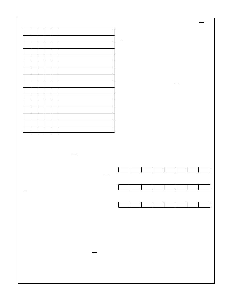
TABLE 6. INTERNAL DATA ACCESS DECODE STARTING BYTE
FSC A3
A2
A1
A0
DESCRIPTION
X
0
0
0
0
Data Output Register, Byte 0
X
0
0
0
1
Data Output Register, Byte 1
X
0
0
1
0
Data Output Register, Byte 2
X
0
1
0
0
Control Register, Byte 0
X
0
1
0
1
Control Register, Byte 1
X
0
1
1
0
Control Register, Byte 2
X
1
0
0
0
Offset Cal Register, Byte 0
X
1
0
0
1
Offset Cal Register, Byte 1
X
1
0
1
0
Offset Cal Register, Byte 2
0
1
1
0
0
Positive Full Scale Cal Register, Byte 0
0
1
1
0
1
Positive Full Scale Cal Register, Byte 1
0
1
1
1
0
Positive Full Scale Cal Register, Byte 2
1
1
1
0
0
Negative Full Scale Cal Register, Byte 0
1
1
1
0
1
Negative Full Scale Cal Register, Byte 1
1
1
1
1
0
Negative Full Scale Cal Register, Byte 2
BYTE 2
MSB
22
21
20
19
18
17
16
D23
D22
D21
D20
D19
D18
D17
D16
BYTE 1
15
14
13
12
11
10
9
8
D15
D14
D13
D12
D11
D10
D9
D8
BYTE 0
7
6
5
4
3
2
1
LSB
D7
D6
D5
D4
D3
D2
D1
D0
HI7190
相關PDF資料 |
PDF描述 |
|---|---|
| HI7190IB | null24-Bit, High Precision, Sigma Delta A/D Converter |
| HIH-3602-A | Humidity Sensor(濕度傳感器) |
| HIH-3602-L-CP | Humidity Sensor(濕度傳感器) |
| HIN240 | 5V High-Speed RS-232 Transceivers with 0.1uF Capacitors |
| HIN240CN | 5V High-Speed RS-232 Transceivers with 0.1uF Capacitors |
相關代理商/技術參數 |
參數描述 |
|---|---|
| HI7190IB | 功能描述:IC ADC 24BIT PROGBL SER 20-SOIC RoHS:否 類別:集成電路 (IC) >> 數據采集 - 模數轉換器 系列:- 產品培訓模塊:Lead (SnPb) Finish for COTS Obsolescence Mitigation Program 標準包裝:2,500 系列:- 位數:12 采樣率(每秒):3M 數據接口:- 轉換器數目:- 功率耗散(最大):- 電壓電源:- 工作溫度:- 安裝類型:表面貼裝 封裝/外殼:SOT-23-6 供應商設備封裝:SOT-23-6 包裝:帶卷 (TR) 輸入數目和類型:- |
| HI7190IBZ | 功能描述:模數轉換器 - ADC ADC 24BIT 10MHZ SIGMADELTA 20 IND RoHS:否 制造商:Texas Instruments 通道數量:2 結構:Sigma-Delta 轉換速率:125 SPs to 8 KSPs 分辨率:24 bit 輸入類型:Differential 信噪比:107 dB 接口類型:SPI 工作電源電壓:1.7 V to 3.6 V, 2.7 V to 5.25 V 最大工作溫度:+ 85 C 安裝風格:SMD/SMT 封裝 / 箱體:VQFN-32 |
| HI7190IBZ-T | 功能描述:模數轉換器 - ADC ADC 24BIT 10MHZ SIGMADELTA 20 IND RoHS:否 制造商:Texas Instruments 通道數量:2 結構:Sigma-Delta 轉換速率:125 SPs to 8 KSPs 分辨率:24 bit 輸入類型:Differential 信噪比:107 dB 接口類型:SPI 工作電源電壓:1.7 V to 3.6 V, 2.7 V to 5.25 V 最大工作溫度:+ 85 C 安裝風格:SMD/SMT 封裝 / 箱體:VQFN-32 |
| HI7190IP | 功能描述:IC ADC 24BIT PROGBL SER 20-PDIP RoHS:否 類別:集成電路 (IC) >> 數據采集 - 模數轉換器 系列:- 產品培訓模塊:Lead (SnPb) Finish for COTS Obsolescence Mitigation Program 標準包裝:2,500 系列:- 位數:12 采樣率(每秒):3M 數據接口:- 轉換器數目:- 功率耗散(最大):- 電壓電源:- 工作溫度:- 安裝類型:表面貼裝 封裝/外殼:SOT-23-6 供應商設備封裝:SOT-23-6 包裝:帶卷 (TR) 輸入數目和類型:- |
| HI7190IPZ | 功能描述:模數轉換器 - ADC W/ANNEAL ADC 24BIT 1 0HZ SIGMADELTA RoHS:否 制造商:Texas Instruments 通道數量:2 結構:Sigma-Delta 轉換速率:125 SPs to 8 KSPs 分辨率:24 bit 輸入類型:Differential 信噪比:107 dB 接口類型:SPI 工作電源電壓:1.7 V to 3.6 V, 2.7 V to 5.25 V 最大工作溫度:+ 85 C 安裝風格:SMD/SMT 封裝 / 箱體:VQFN-32 |
發布緊急采購,3分鐘左右您將得到回復。