- 您現在的位置:買賣IC網 > PDF目錄385382 > HIP6018BCB (HARRIS SEMICONDUCTOR) FPGA - 100000 SYSTEM GATE 2.5 VOLT - NOT RECOMMENDED for NEW DESIGN PDF資料下載
參數資料
| 型號: | HIP6018BCB |
| 廠商: | HARRIS SEMICONDUCTOR |
| 元件分類: | 穩壓器 |
| 英文描述: | FPGA - 100000 SYSTEM GATE 2.5 VOLT - NOT RECOMMENDED for NEW DESIGN |
| 中文描述: | SWITCHING CONTROLLER, 215 kHz SWITCHING FREQ-MAX, PDSO24 |
| 文件頁數: | 11/14頁 |
| 文件大小: | 134K |
| 代理商: | HIP6018BCB |
2-248
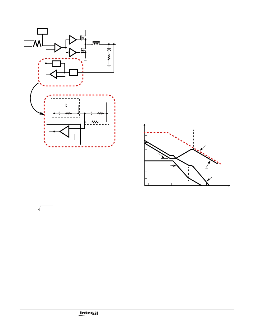
The modulator transfer function is the small-signal transfer
function of V
OUT
/V
E/A
. This function is dominated by a DC
gain and the output filter, with a double pole break frequency
at F
LC
and a zero at F
ESR
. The DC gain of the modulator is
simply the input voltage, V
IN
, divided by the peak-to-peak
oscillator voltage,
V
OSC
.
Modulator Break Frequency Equations
The compensation network consists of the error amplifier
internal to the HIP6018B and the impedance networks Z
IN
and
Z
FB
. The goal of the compensation network is to provide a
closed loop transfer function with an acceptable 0dB crossing
frequency (f
0dB
) and adequate phase margin. Phase margin is
the difference between the closed loop phase at f
0dB
and 180
degrees
.
The equations below relate the compensation
network’s poles, zeros and gain to the components (R1, R2,
R3, C1, C2, and C3) in Figure 11. Use these guidelines for
locating the poles and zeros of the compensation network:
1. Pick Gain (R2/R1) for desired converter bandwidth
2. Place 1
ST
Zero Below Filter’s Double Pole (~75% F
LC
)
3. Place 2
ND
Zero at Filter’s Double Pole
4. Place 1
ST
Pole at the ESR Zero
5. Place 2
ND
Pole at Half the Switching Frequency
6. Check Gain against Error Amplifier’s Open-Loop Gain
7. Estimate Phase Margin - Repeat if Necessary
Compensation Break Frequency Equations
Figure 12 shows an asymptotic plot of the DC-DC converter’s
gain vs. frequency. The actual modulator gain has a peak due
to the high Q factor of the output filter at F
LC
, which is not
shown in Figure 12. Using the above guidelines should yield a
compensation gain similar to the curve plotted. The open loop
error amplifier gain bounds the compensation gain. Check the
compensation gain at F
P2
with the capabilities of the error
amplifier. The closed loop gain is constructed on the log-log
graph of Figure 12 by adding the modulator gain (in dB) to the
compensation gain (in dB). This is equivalent to multiplying
the modulator transfer function to the compensation transfer
function and plotting the gain.
The compensation gain uses external impedance networks
Z
FB
and Z
IN
to provide a stable, high bandwidth loop. A
stable control loop has a 0dB gain crossing with
-20dB/decade slope and a phase margin greater than 45
degrees. Include worst case component variations when
determining phase margin.
Component Selection Guidelines
Output Capacitor Selection
The output capacitors for each output have unique
requirements. In general the output capacitors should be
selected to meet the dynamic regulation requirements.
Additionally, the PWM converters require an output capacitor
to filter the current ripple. The linear regulator is internally
compensated and requires an output capacitor that meets
the stability requirements. The load transient for the
microprocessor core requires high quality capacitors to
supply the high slew rate (di/dt) current demands.
FIGURE 11. VOLTAGE-MODE BUCK CONVERTER
COMPENSATION DESIGN
V
OUT
OSC
REFERENCE
L
O
C
O
ESR
V
IN
V
OSC
ERROR
AMP
PWM
COMP
-
DRIVER
(PARASITIC)
Z
FB
+
-
REFERENCE
R1
R3
R2
C3
C2
C1
COMP
V
OUT
FB
Z
FB
HIP6018B
Z
IN
DRIVER
DETAILED FEEDBACK COMPENSATION
PHASE
V
E/A
+
+
-
Z
IN
F
LC
L
O
2
π
C
O
×
×
---------------------------------------
=
F
ESR
O
-----------------------------------------
=
F
Z1
-----------------------------------
=
F
Z2
R3
)
C3
×
------------------------+
=
F
P1
2
π
R
2
--------+
×
×
------------------------------------------------------
=
F
P2
-----------------------------------
=
100
80
60
40
20
0
-20
-40
-60
F
P1
F
Z2
10M
1M
100K
10K
1K
100
10
OPEN LOOP
ERROR AMP GAIN
F
Z1
F
P2
20LOG
(R
2
/R
1
)
F
LC
F
ESR
COMPENSATION
GAIN
G
FREQUENCY (Hz)
20LOG
(V
IN
/
V
OSC
)
MODULATOR
GAIN
FIGURE 12. ASYMPTOTIC BODE PLOT OF CONVERTER GAIN
CLOSED LOOP
GAIN
HIP6018B
相關PDF資料 |
PDF描述 |
|---|---|
| HIP6019 | FPGA - 100000 SYSTEM GATE 2.5 VOLT - NOT RECOMMENDED for NEW DESIGN |
| HIP6019CB | Advanced Dual PWM and Dual Linear Power Control |
| HIP6019EVAL1 | Advanced Dual PWM and Dual Linear Power Control |
| HIP6019 | 5-BIT PROGRAMMABLE SYNCHRONOUS BUCK, NON-SYNCHRONOUS,ADJUSTABLE LDO AND 200mA ON-BOARD LDO |
| HIP6020A | Advanced Dual PWM and Dual Linear Power Controller |
相關代理商/技術參數 |
參數描述 |
|---|---|
| HIP6018BCB-T | 功能描述:IC REG TRPL BCK/LINEAR 24-SOIC RoHS:否 類別:集成電路 (IC) >> PMIC - 穩壓器 - 線性 + 切換式 系列:- 標準包裝:2,500 系列:- 拓撲:降壓(降壓)同步(3),線性(LDO)(2) 功能:任何功能 輸出數:5 頻率 - 開關:300kHz 電壓/電流 - 輸出 1:控制器 電壓/電流 - 輸出 2:控制器 電壓/電流 - 輸出 3:控制器 帶 LED 驅動器:無 帶監控器:無 帶序列發生器:是 電源電壓:5.6 V ~ 24 V 工作溫度:-40°C ~ 85°C 安裝類型:* 封裝/外殼:* 供應商設備封裝:* 包裝:* |
| HIP6018BCBZ | 功能描述:電壓模式 PWM 控制器 ADV DL PWM "3 IN1" W/LWER DAC RNG RoHS:否 制造商:Texas Instruments 輸出端數量:1 拓撲結構:Buck 輸出電壓:34 V 輸出電流: 開關頻率: 工作電源電壓:4.5 V to 5.5 V 電源電流:600 uA 最大工作溫度:+ 125 C 最小工作溫度:- 40 C 封裝 / 箱體:WSON-8 封裝:Reel |
| HIP6018BCBZ-T | 功能描述:電壓模式 PWM 控制器 ADV DL PWM "3 IN1" W/LWER DAC RNG RoHS:否 制造商:Texas Instruments 輸出端數量:1 拓撲結構:Buck 輸出電壓:34 V 輸出電流: 開關頻率: 工作電源電壓:4.5 V to 5.5 V 電源電流:600 uA 最大工作溫度:+ 125 C 最小工作溫度:- 40 C 封裝 / 箱體:WSON-8 封裝:Reel |
| HIP6018CB | 制造商:Rochester Electronics LLC 功能描述:- Bulk 制造商:Harris Corporation 功能描述: |
| HIP6018CB-T | 制造商:Rochester Electronics LLC 功能描述:- Tape and Reel |
發布緊急采購,3分鐘左右您將得到回復。