- 您現在的位置:買賣IC網 > PDF目錄385382 > HIP6019CB (HARRIS SEMICONDUCTOR) Advanced Dual PWM and Dual Linear Power Control PDF資料下載
參數資料
| 型號: | HIP6019CB |
| 廠商: | HARRIS SEMICONDUCTOR |
| 元件分類: | 穩壓器 |
| 英文描述: | Advanced Dual PWM and Dual Linear Power Control |
| 中文描述: | DUAL SWITCHING CONTROLLER, 215 kHz SWITCHING FREQ-MAX, PDSO28 |
| 文件頁數: | 7/15頁 |
| 文件大小: | 152K |
| 代理商: | HIP6019CB |
2-258
FB4 (Pin 14)
Connect this pin to a resistor divider to set the linear
regulator output.
Description
Operation
The HIP6019 monitors and precisely controls 4 output
voltage levels (Refer to Figures 1, 2, and 3). It is designed for
microprocessor computer applications with 5V power and
12V bias input from a PS2 or ATX power supply. The IC has
2 PWM controllers, a linear controller, and a linear regulator.
The first PWM controller (PWM1) is designed to regulate the
microprocessor core voltage (V
OUT1
). PWM1 controller
drives 2 MOSFETs (Q1 and Q2) in a synchronous-rectified
buck converter configuration and regulates the core voltage
to a level programmed by the 5-bit digital-to-analog
converter (DAC). The second PWM controller (PWM2) is
designed to regulate the I/O voltage (V
OUT2
). PWM2
controller drives a MOSFET (Q3) in a standard buck
converter configuration and regulates the I/O voltage to a
resistor programmable level between 3.0 and 3.5V
DC
. An
integrated linear regulator supplies the 2.5V clock generator
power (V
OUT4
). The linear controller drives an external
MOSFET (Q4) to supply the GTL bus power (V
OUT3
).
Initialization
The HIP6019 automatically initializes upon receipt of input
power. Special sequencing of the input supplies is not
necessary. The Power-On Reset (POR) function continually
monitors the input supply voltages. The POR monitors the
bias voltage (+12V
IN
) at the VCC pin and the 5V input voltage
(+5V
IN
) at the OCSET1 pin. The normal level on OCSET1 is
equal to +5V
IN
less a fixed voltage drop (see over-current
protection). The POR function initiates soft-start operation
after both input supply voltages exceed their POR thresholds.
Soft-Start
The POR function initiates the soft-start sequence. Initially,
the voltage on the SS pin rapidly increases to approximately
1V (this minimizes the soft-start interval). Then an internal
11
μ
A current source charges an external capacitor (C
SS
) on
the SS pin to 4V. The PWM error amplifier reference inputs
(+ terminal) and outputs (COMP1 and COMP2 pins) are
clamped to a level proportional to the SS pin voltage. As the
SS pin voltage ramps from 1V to 4V, the output clamp allows
generation of PHASE pulses of increasing width that charge
the output capacitor(s). After this initial stage, the reference
input clamp slows the output voltage rate-of-rise and
provides a smooth transition to the final set voltage.
Additionally, both linear regulator’s reference inputs are
clamped to a voltage proportional to the SS pin voltage. This
method provides a rapid and controlled output voltage rise.
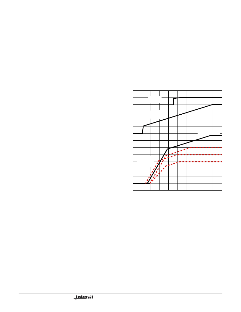
Figure 6 shows the soft-start sequence for the typical
application. At T0 the SS voltage rapidly increases to
approximately 1V. At T1, the SS pin and error amplifier output
voltage reach the valley of the oscillator’s triangle wave. The
oscillator’s triangular waveform is compared to the clamped
error amplifier output voltage. As the SS pin voltage
increases, the pulse-width on the PHASE pin increases. The
interval of increasing pulse-width continues until each output
reaches sufficient voltage to transfer control to the input
reference clamp. If we consider the 3.3V output (V
OUT2
) in
Figure 6, this time occurs at T2. During the interval between
T2 and T3, the error amplifier reference ramps to the final
value and the converter regulates the output to a voltage
proportional to the SS pin voltage. At T3 the input clamp
voltage exceeds the reference voltage and the output voltage
is in regulation.
The remaining outputs are also programmed to follow the SS
pin voltage. Each linear output (V
OUT3
and V
OUT4
) initially
follows the 3.3V output (V
OUT2
). When each output reaches
sufficient voltage the input reference clamp slows the rate of
output voltage rise. The PGOOD signal toggles ‘high’ when
all output voltage levels have exceeded their under-voltage
levels. See the Soft-Start Interval section under Applications
Guidelines for a procedure to determine the soft-start interval.
Fault Protection
All four outputs are monitored and protected against extreme
overload. A sustained overload on any linear regulator
output or an over-voltage on the PWM outputs disables all
converters and drives the FAULT/RT pin to VCC.
Figure 7 shows a simplified schematic of the fault logic. An
over-voltage detected on either VSEN1 or VSEN2
FIGURE 6. SOFT-START INTERVAL
0V
0V
0V
TIME
PGOOD
(2V/DIV)
SOFT-START
(1V/DIV)
OUTPUT
VOLTAGES
(0.5V/DIV)
V
OUT1
(DAC = 2V)
V
OUT2
(= 3.3V)
V
OUT4
(= 2.5V)
V
OUT3
( = 1.5V)
T1
T2
T3
T0
HIP6019
相關PDF資料 |
PDF描述 |
|---|---|
| HIP6019EVAL1 | Advanced Dual PWM and Dual Linear Power Control |
| HIP6019 | 5-BIT PROGRAMMABLE SYNCHRONOUS BUCK, NON-SYNCHRONOUS,ADJUSTABLE LDO AND 200mA ON-BOARD LDO |
| HIP6020A | Advanced Dual PWM and Dual Linear Power Controller |
| HIP6020ACB | Advanced Dual PWM and Dual Linear Power Controller |
| HIP6020EVAL1 | Advanced Dual PWM and Dual Linear Power Controller |
相關代理商/技術參數 |
參數描述 |
|---|---|
| HIP6019CB-T | 制造商:Rochester Electronics LLC 功能描述:- Bulk |
| HIP6019EVAL1 | 制造商:INTERSIL 制造商全稱:Intersil Corporation 功能描述:Advanced Dual PWM and Dual Linear Power Control |
| HIP6020 | 制造商:INTERSIL 制造商全稱:Intersil Corporation 功能描述:Advanced Dual PWM and Dual Linear Power Controller |
| HIP6020A | 制造商:INTERSIL 制造商全稱:Intersil Corporation 功能描述:Advanced Dual PWM and Dual Linear Power Controller |
| HIP6020A_01 | 制造商:INTERSIL 制造商全稱:Intersil Corporation 功能描述:Advanced Dual PWM and Dual Linear Power Controller |
發布緊急采購,3分鐘左右您將得到回復。