- 您現在的位置:買賣IC網 > Datasheet目錄40 > HIP6021CB-T (Intersil)IC REG QD BCK/LINEAR 28-SOIC Datasheet資料下載
參數資料
| 型號: | HIP6021CB-T |
| 廠商: | Intersil |
| 文件頁數: | 12/15頁 |
| 文件大小: | 408K |
| 描述: | IC REG QD BCK/LINEAR 28-SOIC |
| 標準包裝: | 1,000 |
| 拓撲: | 降壓(降壓)同步(1),線性(LDO)(3) |
| 功能: | 任何功能 |
| 輸出數: | 4 |
| 頻率 - 開關: | 215kHz |
| 電壓/電流 - 輸出 1: | 控制器 |
| 電壓/電流 - 輸出 2: | 控制器 |
| 電壓/電流 - 輸出 3: | 控制器 |
| 帶 LED 驅動器: | 無 |
| 帶監控器: | 無 |
| 帶序列發生器: | 無 |
| 電源電壓: | 5 V ~ 12 V |
| 工作溫度: | 0°C ~ 70°C |
| 安裝類型: | * |
| 封裝/外殼: | 28-SOIC(0.295",7.50mm 寬) |
| 供應商設備封裝: | * |
| 包裝: | 帶卷 (TR) |
12
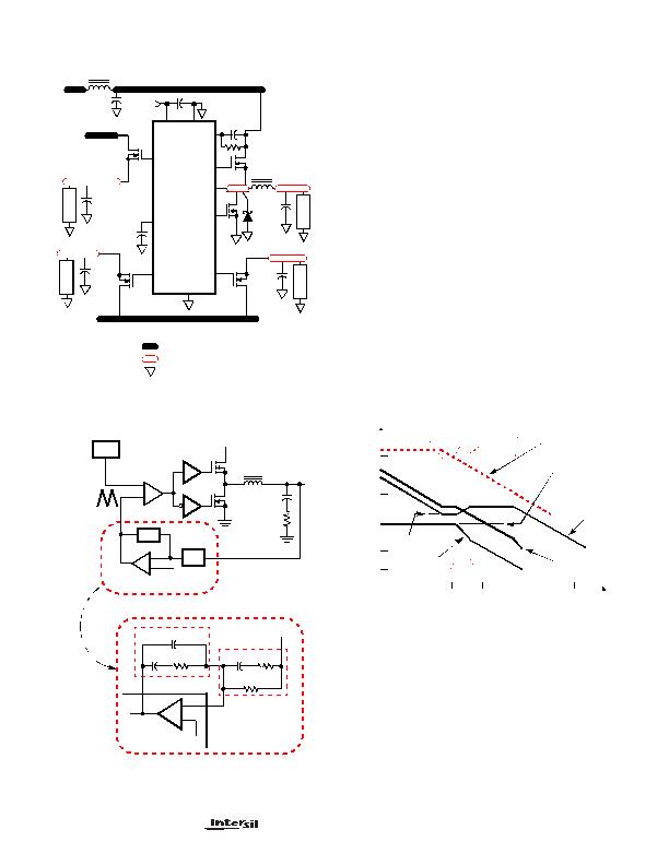
Compensation Break Frequency Equations
Figure 10 shows an asymptotic plot of the DC-DC
converters gain vs. frequency. The actual Modulator Gain
has a high gain peak dependent on the quality factor (Q) of
the output filter, which is not shown in Figure 9. Using the
above guidelines should yield a Compensation Gain similar
to the curve plotted. The open loop error amplifier gain
bounds the compensation gain. Check the compensation
gain at F
P2
with the capabilities of the error amplifier. The
Closed Loop Gain is constructed on the log-log graph of
Figure 10 by adding the Modulator Gain (in dB) to the
Compensation Gain (in dB). This is equivalent to multiplying
the modulator transfer function to the compensation transfer
function and plotting the gain.
The compensation gain uses external impedance networks
Z
FB
and Z
IN
to provide a stable, high bandwidth (BW) overall
loop. A stable control loop has a gain crossing with
-20dB/decade slope and a phase margin greater than 45
degrees. Include worst case component variations when
determining phase margin.
Component Selection Guidelines
Output Capacitor Selection
The output capacitors for each output have unique
requirements. In general, the output capacitors should be
selected to meet the dynamic regulation requirements.
Additionally, the PWM converters require an output capacitor
to filter the current ripple. The load transient for the
microprocessor core requires high quality capacitors to
supply the high slew rate (di/dt) current demands.
FIGURE 8. PRINTED CIRCUIT BOARD POWER PLANES AND
ISLANDS
V
OUT1
Q1
Q2
Q3
Q4
C
SS
+12V
C
VCC
VIA CONNECTION TO GROUND PLANE
ISLAND ON POWER PLANE LAYER
ISLAND ON CIRCUIT PLANE LAYER
L
OUT1
C
OUT1
CR1
HIP6021
C
IN
C
OUT2
V
OUT2
V
OUT3
+5V
IN
SS
PGND
LGATE1
UGATE1
PHASE1
DRIVE3
KEY
GND
VCC
DRIVE2
OCSET1
R
OCSET1
C
OCSET1
V
OUT4
DRIVE4
+3.3V
IN
L
IN
Q5
C
OUT3
C
OUT4
+3.3V
IN
FIGURE 9. VOLTAGE-MODE BUCK CONVERTER
COMPENSATION DESIGN
V
OUT
OSC
REFERENCE
L
O
C
O
ESR
V
IN
V
OSC
ERROR
AMP
PWM
DRIVER
(PARASITIC)
Z
FB
+
-
DACOUT
R1
R3
R2
C3
C2
C1
COMP
V
OUT
FB
Z
FB
HIP6021
Z
IN
COMP
DRIVER
DETAILED COMPENSATION COMPONENTS
PHASE
V
E/A
+
-
+
-
Z
IN
F
Z1
1
2?nbsp R
?nbsp 2 C1
?/DIV>
-----------------------------------
=
F
Z2
1
2?nbsp R1 R3
+
(
) C3
?/DIV>
?/DIV>
------------------------------------------------------ -
=
F
P1
1
2?nbsp R
2
C1 C2
?/DIV>
C1 C2
+
--------------------- -
?/DIV>
?/DIV>
?/DIV>
?/DIV>
?/DIV>
?/DIV>
------------------------------------------------------ -
=
F
P2
1
2?nbsp R
?nbsp 3 C3
?/DIV>
-----------------------------------
=
FIGURE 10. ASYMPTOTIC BODE PLOT OF CONVERTER GAIN
100
80
60
40
20
0
-20
-40
-60
F
P1
F
Z2
10M
1M
100K
10K
1K
100
10
OPEN LOOP
ERROR AMP GAIN
F
Z1
F
P2
F
LC
F
ESR
COMPENSATION
FREQUENCY (Hz)
GAIN
MODULATOR
GAIN
CLOSED LOOP
GAIN
20
V
IN
V
PP
------------
?/DIV>
?/DIV>
?/DIV>
?/DIV>
主站蜘蛛池模板:
建阳市|
安康市|
新余市|
高碑店市|
霍城县|
冕宁县|
秦皇岛市|
丹寨县|
靖安县|
石楼县|
临江市|
东兰县|
泽普县|
乌鲁木齐县|
陕西省|
彰武县|
隆尧县|
江津市|
江门市|
太仆寺旗|
乌兰察布市|
安达市|
舒城县|
吕梁市|
中宁县|
襄垣县|
凤翔县|
连平县|
灵山县|
宣威市|
姚安县|
龙里县|
五河县|
泗洪县|
永仁县|
潼南县|
上杭县|
尉氏县|
香河县|
大埔区|
通辽市|
?/DIV>
?/DIV>
log
20
R2
R1
------- -
?nbsp ?/DIV>
?nbsp ?/DIV>
log
HIP6021
相關PDF資料 |
PDF描述 |
|---|---|
| HIP6521CB-T | IC REG QD BCK/LINEAR SYNC 16SOIC |
| HMC920LP5E | IC CTRLR ACTIVE BIAS 32QFN |
| IDTTSE2002B3CNRG | IC TEMP SENS EEPROM DFN-8 |
| IPM6220ACAZ-T | IC REG 5OUT BUCK/LDO SYNC 24SSOP |
| IR2170 | IC CURRENT SENSE 600V 1MA 8-DIP |
相關代理商/技術參數 |
參數描述 |
|---|---|
| HIP6021CBZ | 功能描述:電壓模式 PWM 控制器 SINGLE PWM & TRPL LINEAR CNTRLR RoHS:否 制造商:Texas Instruments 輸出端數量:1 拓撲結構:Buck 輸出電壓:34 V 輸出電流: 開關頻率: 工作電源電壓:4.5 V to 5.5 V 電源電流:600 uA 最大工作溫度:+ 125 C 最小工作溫度:- 40 C 封裝 / 箱體:WSON-8 封裝:Reel |
| HIP6021CBZ-T | 功能描述:電壓模式 PWM 控制器 SINGLE PWM & TRPL LINEAR CNTRLR RoHS:否 制造商:Texas Instruments 輸出端數量:1 拓撲結構:Buck 輸出電壓:34 V 輸出電流: 開關頻率: 工作電源電壓:4.5 V to 5.5 V 電源電流:600 uA 最大工作溫度:+ 125 C 最小工作溫度:- 40 C 封裝 / 箱體:WSON-8 封裝:Reel |
| HIP6021EVAL1 | 功能描述:電源管理IC開發工具 HIP6021 EVAL BRD RoHS:否 制造商:Maxim Integrated 產品:Evaluation Kits 類型:Battery Management 工具用于評估:MAX17710GB 輸入電壓: 輸出電壓:1.8 V |
| HIP6028 | 制造商:INTERSIL 制造商全稱:Intersil Corporation 功能描述:Advanced PWM and Dual Linear Power Control with Integrated ACPI Support Interface |
| HIP6028CB | 制造商:Rochester Electronics LLC 功能描述:- Bulk |
發布緊急采購,3分鐘左右您將得到回復。