- 您現在的位置:買賣IC網 > Datasheet目錄40 > HIP6521CB-T (Intersil)IC REG QD BCK/LINEAR SYNC 16SOIC Datasheet資料下載
參數資料
| 型號: | HIP6521CB-T |
| 廠商: | Intersil |
| 文件頁數: | 11/13頁 |
| 文件大小: | 356K |
| 描述: | IC REG QD BCK/LINEAR SYNC 16SOIC |
| 標準包裝: | 2,500 |
| 拓撲: | 降壓(降壓)同步(1),線性(LDO)(3) |
| 功能: | 任何功能 |
| 輸出數: | 4 |
| 頻率 - 開關: | 300kHz |
| 電壓/電流 - 輸出 1: | 控制器 |
| 電壓/電流 - 輸出 2: | 控制器 |
| 電壓/電流 - 輸出 3: | 控制器 |
| 帶 LED 驅動器: | 無 |
| 帶監控器: | 無 |
| 帶序列發生器: | 無 |
| 電源電壓: | 4.75 V ~ 5.25 V |
| 工作溫度: | 0°C ~ 70°C |
| 安裝類型: | * |
| 封裝/外殼: | 16-SOIC(0.154",3.90mm 寬) |
| 供應商設備封裝: | * |
| 包裝: | 帶卷 (TR) |
11
FN4837.5
October 16, 2006
Use a mix of input bypass capacitors to control the voltage
overshoot across the MOSFETs. Use ceramic capacitance
for the high frequency decoupling and bulk capacitors to
supply the RMS current. Small ceramic capacitors can be
placed very close to the upper MOSFET to suppress the
voltage induced in the parasitic circuit impedances.
For a through-hole design, several electrolytic capacitors
may be needed. For surface mount designs, solid tantalum
capacitors can be used, but caution must be exercised with
regard to the capacitor surge current rating. These
capacitors must be capable of handling the surge-current at
power-up.
Transistors Selection/Considerations
The HIP6521 requires 5 external transistors. Two N-channel
MOSFETs are used in the synchronous-rectified buck
topology of PWM converter. The clock, AGP and MCH/ICH
linear controllers each drive an NPN bipolar transistor as a
pass element. All these transistors should be selected based
upon r
DS(ON)
, current gain, saturation voltages, gate/base
supply requirements, and thermal management
considerations.
PWM MOSFET Selection and Considerations
In high-current PWM applications, the MOSFET power
dissipation, package selection and heatsink are the
dominant design factors. The power dissipation includes two
loss components; conduction loss and switching loss. These
losses are distributed between the upper and lower
MOSFETs according to duty factor (see the equations
below). The conduction losses are the main component of
power dissipation for the lower MOSFETs. Only the upper
MOSFET has significant switching losses, since the lower
device turns on and off into near zero voltage.
The equations below assume linear voltage-current
transitions and do not model power loss due to the reverse-
recovery of the lower MOSFETs body diode. The gate-
charge losses are dissipated by the HIP6521 and don't heat
the MOSFETs. However, large gate-charge increases the
switching time, t
SW
which increases the upper MOSFET
switching losses. Ensure that both MOSFETs are within their
maximum junction temperature at high ambient temperature
by calculating the temperature rise according to package
thermal-resistance specifications. A separate heatsink may
be necessary depending upon MOSFET power, package
type, ambient temperature and air flow.
Given the reduced available gate bias voltage (5V) logic-
level or sub-logic-level transistors have to be used for both
N-MOSFETs. Caution should be exercised with devices
exhibiting very low V
GS(ON)
characteristics, as the low gate
threshold could be conducive to some shoot-through (due to
the Miller effect), in spite of the counteracting circuitry
present aboard the HIP6521.
Rectifier CR1 is a clamp that catches the negative inductor
swing during the dead time between the turn off of the lower
MOSFET and the turn on of the upper MOSFET. The diode
must be a Schottky type to prevent the lossy parasitic
MOSFET body diode from conducting. It is acceptable to
omit the diode and let the body diode of the lower MOSFET
clamp the negative inductor swing, providing the body diode
is fast enough to avoid excessive negative voltage swings at
the PHASE pin. The diode's rated reverse breakdown
voltage must be greater than the maximum input voltage.
Linear Controllers Transistor Selection
The main criteria for selection of transistors for the linear
regulators is package selection for efficient removal of heat.
The power dissipated in a linear regulator is:
Select a package and heatsink that maintains the junction
temperature below the rating with a the maximum expected
ambient temperature.
As bipolar NPN transistors have to be used with the linear
controllers, insure the current gain at the given operating
V
CE
is sufficiently large to provide the desired maximum
output load current when the base is fed with the minimum
driver output current.
P
UPPER
I
O
2
r
DS ON
( )
?/DIV>
V
OUT
?/DIV>
V
IN
----------------------------------------------------------- -
I
O
V
IN
?/DIV>
t
SW
?/DIV>
主站蜘蛛池模板:
岳阳县|
临颍县|
巨鹿县|
常州市|
建水县|
乌兰察布市|
唐河县|
离岛区|
达日县|
清苑县|
筠连县|
辽源市|
云龙县|
三台县|
唐山市|
金乡县|
乌拉特中旗|
兴安盟|
海林市|
开阳县|
广元市|
通海县|
托克托县|
邓州市|
漳浦县|
贞丰县|
山西省|
连云港市|
常德市|
苏尼特左旗|
桂平市|
通江县|
贵阳市|
濮阳市|
武鸣县|
霞浦县|
安平县|
眉山市|
乡宁县|
嘉黎县|
东乌|
F
S
?/DIV>
2
----------------------------------------------------
+
=
P
LOWER
I
O
2
r
DS ON
( )
?/DIV>
V
IN
V
OUT
(
)
?/DIV>
V
IN
-------------------------------------------------------------------------------- -
=
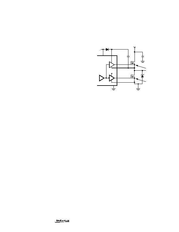
FIGURE 8. MOSFET GATE BIAS
+5V
PGND
HIP6521
GND
LGATE
UGATE
PHASE
BOOT
+5V OR LESS
NOTE:
NOTE:
V
GS
H V
CC
Q1
Q2
+
-
V
GS
H V
CC
-0.5V
CR1
VCC
C
BOOT
VCC
+
P
LINEAR
I
O
V
IN
V
OUT
(
)
?/DIV>
=
HIP6521
相關PDF資料 |
PDF描述 |
|---|---|
| HMC920LP5E | IC CTRLR ACTIVE BIAS 32QFN |
| IDTTSE2002B3CNRG | IC TEMP SENS EEPROM DFN-8 |
| IPM6220ACAZ-T | IC REG 5OUT BUCK/LDO SYNC 24SSOP |
| IR2170 | IC CURRENT SENSE 600V 1MA 8-DIP |
| IR2171STR | IC CURRENT SENSE 8SOIC |
相關代理商/技術參數 |
參數描述 |
|---|---|
| HIP6521CBZ | 功能描述:電壓模式 PWM 控制器 4 IN 1 PWM/LINEAR CNTRLR 5V RoHS:否 制造商:Texas Instruments 輸出端數量:1 拓撲結構:Buck 輸出電壓:34 V 輸出電流: 開關頻率: 工作電源電壓:4.5 V to 5.5 V 電源電流:600 uA 最大工作溫度:+ 125 C 最小工作溫度:- 40 C 封裝 / 箱體:WSON-8 封裝:Reel |
| HIP6521CBZA | 功能描述:IC REG QD BCK/LINEAR 16-SOIC RoHS:是 類別:集成電路 (IC) >> PMIC - 穩壓器 - 線性 + 切換式 系列:- 標準包裝:2,500 系列:- 拓撲:降壓(降壓)同步(3),線性(LDO)(2) 功能:任何功能 輸出數:5 頻率 - 開關:300kHz 電壓/電流 - 輸出 1:控制器 電壓/電流 - 輸出 2:控制器 電壓/電流 - 輸出 3:控制器 帶 LED 驅動器:無 帶監控器:無 帶序列發生器:是 電源電壓:5.6 V ~ 24 V 工作溫度:-40°C ~ 85°C 安裝類型:* 封裝/外殼:* 供應商設備封裝:* 包裝:* |
| HIP6521CBZA-T | 功能描述:IC REG QD BCK/LINEAR 16-SOIC RoHS:是 類別:集成電路 (IC) >> PMIC - 穩壓器 - 線性 + 切換式 系列:- 標準包裝:2,500 系列:- 拓撲:降壓(降壓)同步(3),線性(LDO)(2) 功能:任何功能 輸出數:5 頻率 - 開關:300kHz 電壓/電流 - 輸出 1:控制器 電壓/電流 - 輸出 2:控制器 電壓/電流 - 輸出 3:控制器 帶 LED 驅動器:無 帶監控器:無 帶序列發生器:是 電源電壓:5.6 V ~ 24 V 工作溫度:-40°C ~ 85°C 安裝類型:* 封裝/外殼:* 供應商設備封裝:* 包裝:* |
| HIP6521CBZ-T | 功能描述:電壓模式 PWM 控制器 4 IN 1 PWM/LINEAR CNTRLR 5V RoHS:否 制造商:Texas Instruments 輸出端數量:1 拓撲結構:Buck 輸出電壓:34 V 輸出電流: 開關頻率: 工作電源電壓:4.5 V to 5.5 V 電源電流:600 uA 最大工作溫度:+ 125 C 最小工作溫度:- 40 C 封裝 / 箱體:WSON-8 封裝:Reel |
| HIP6521EVAL1 | 功能描述:電源管理IC開發工具 HIP6521 PWM & TRPL L LINEAR CNT EVAL BRD RoHS:否 制造商:Maxim Integrated 產品:Evaluation Kits 類型:Battery Management 工具用于評估:MAX17710GB 輸入電壓: 輸出電壓:1.8 V |
發布緊急采購,3分鐘左右您將得到回復。