- 您現在的位置:買賣IC網 > PDF目錄371841 > HM6288JP-25 x4 SRAM PDF資料下載
參數資料
| 型號: | HM6288JP-25 |
| 英文描述: | x4 SRAM |
| 中文描述: | x4的SRAM |
| 文件頁數: | 1/1頁 |
| 文件大小: | 60K |
| 代理商: | HM6288JP-25 |
date: 2002/10/04
1/1
HITACHI SEMICONDUCTOR TECHNICAL UPDATE
Classification
of Production
Memory
No
TN-M62-112A/E
Rev
1
THEME
SRAM: Notes on Usage
Classification of
Information
1.
2.
3.
4.
5. Change of Production Line
Spec change
Supplement of Documents
Limitation of Use
Change of Mask
Lot No.
Effective Date
PRODUCT
NAME
All 4-Mbit fast
SRAM C-mask
products
All Lots
Reference
Documents
Hitachi IC memory datasheets
ADE-203-1196B(Z)/1198B(Z)/1199B(Z)/
1200C(Z)/1294D(Z)/1202C(Z)/1263A(Z)
/1283A(Z)/1304A(Z)/1305A(Z)
Permanent
As the operating speeds of SRAM products rise, securing the various design margins is becoming more
difficult. Accordingly, there is an increasing possibility of noise from the input-signal or power-supply
lines acting as an obstacle to the normal operation of SRAM products. To prevent malfunctions in 4-Mbit
fast SRAM (C-mask) products, please note the following points.
1.
Announcement
In executing a write-with-verify operations with a 4-Mbit fast SRAM (C-mask) product, incorrect data
may be read because of noise, etc., even when the data has been written correctly (see figure 1 and note
1). This problem does not arise with a further read operation. If you are having problems of the type
described or your project may be subject to such problems, refer to the points below for the appropriate
countermeasures.
2.
Countermeasures
Please apply countermeasures (1) and (2) below according to your situation.
(1)
Avoid executing the read for verification in the same cycle as the write operation it follows. Verify the
written data after inputting an address or switching the /CS signal.
(2)
Please ensure that your design is not subject to adverse effects because of distortion or skewing of the
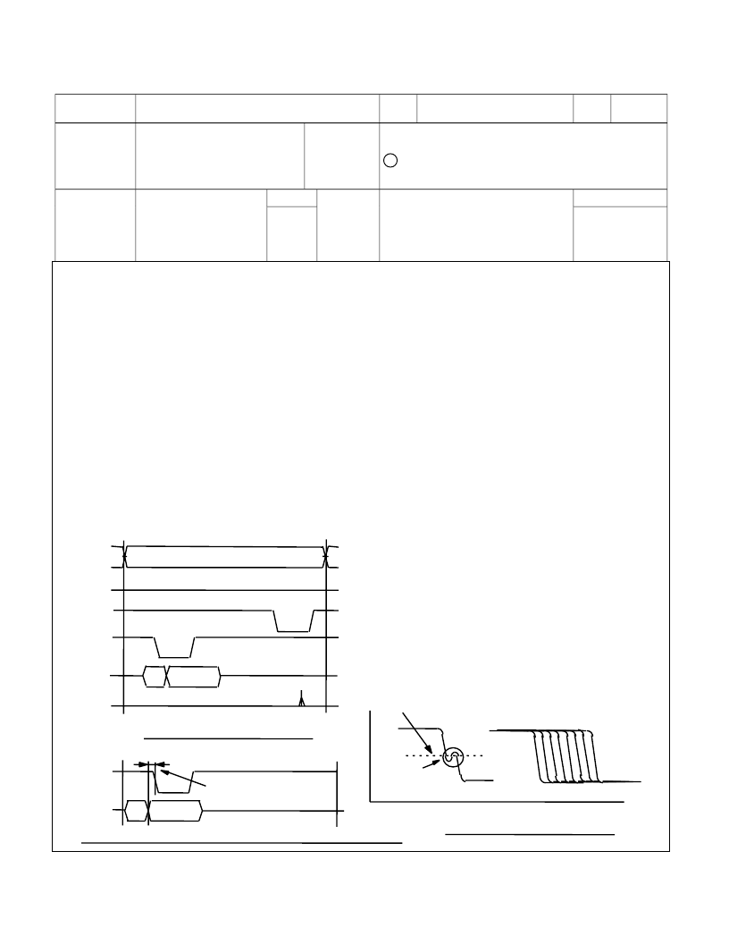
Din input waveform (figure 2). Drive /WE low (write) after determining the data on Din (see figure 3).
Time
Din waveform skew
Figure 2 Din Input Waveform
Distortion of input waveform
Input threshold voltage
*1:
Write verify : After data is written within the same
address cycle, perform data-read operation.
Figure 1. Write Verify Timing
ADD
/CS
/WE
Din
STRB
Fixed to a low level
/D
D
Read operation
/OE
/WE
Din
/D
D
After the Din data is
determined, drive /WE low.
Figure 3 Write Verify Timing (Countermeasure Applied)
V
相關PDF資料 |
PDF描述 |
|---|---|
| HM6288JP-35 | x4 SRAM |
| HM6288JP-45 | x4 SRAM |
| HM6288LJP-25 | x4 SRAM |
| HM6288LJP-35 | x4 SRAM |
| HM6288LP-25 | x4 SRAM |
相關代理商/技術參數 |
參數描述 |
|---|---|
| HM6288JP-35 | 制造商:未知廠家 制造商全稱:未知廠家 功能描述:x4 SRAM |
| HM6288JP-45 | 制造商:未知廠家 制造商全稱:未知廠家 功能描述:x4 SRAM |
| HM6288LJP-25 | 制造商:未知廠家 制造商全稱:未知廠家 功能描述:x4 SRAM |
| HM6288LJP-35 | 制造商:未知廠家 制造商全稱:未知廠家 功能描述:x4 SRAM |
| HM6288LP-25 | 制造商:未知廠家 制造商全稱:未知廠家 功能描述:x4 SRAM |
發布緊急采購,3分鐘左右您將得到回復。