- 您現在的位置:買賣IC網 > PDF目錄385388 > HMP8116CN (HARRIS SEMICONDUCTOR) NTSC/PAL Video Decoder PDF資料下載
參數資料
| 型號: | HMP8116CN |
| 廠商: | HARRIS SEMICONDUCTOR |
| 元件分類: | 顏色信號轉換 |
| 英文描述: | NTSC/PAL Video Decoder |
| 中文描述: | COLOR SIGNAL DECODER, PQFP80 |
| 文件頁數: | 14/43頁 |
| 文件大小: | 182K |
| 代理商: | HMP8116CN |
第1頁第2頁第3頁第4頁第5頁第6頁第7頁第8頁第9頁第10頁第11頁第12頁第13頁當前第14頁第15頁第16頁第17頁第18頁第19頁第20頁第21頁第22頁第23頁第24頁第25頁第26頁第27頁第28頁第29頁第30頁第31頁第32頁第33頁第34頁第35頁第36頁第37頁第38頁第39頁第40頁第41頁第42頁第43頁
14
8-BIT BT.656 OUTPUT
If BT.656 data is generated, it is output following each rising
edge of CLK2. The BT.656 EAV and SAV formats are shown
in Table 4 and the pixel output timing is shown in Figure 15.
The EAV and SAV timing is determined by the programmed
horizontal and vertical blank timing
BLANK, HSYNC, VSYNC, DVALID, VBIVALID, and FIELD
are output following the rising edge of CLK2.
For proper operation, CLK2 must be exactly 2x the desired
output sample rate. The DVALID output is continuously
asserted during the entire active video time.
During the blanking intervals, the YCbCr outputs have a
value of 16 for Y and 128 for Cb and Cr, unless ancillary data
is present.
Due to the use of digital PLLs and source video timing the
total # of samples per line may not equal exactly 1716
(NTSC) or 1728 (PAL). The active video portion of the
BT.656 data stream is always exactly 1440 continous sam-
ples. Any line-to-line timing difference from nominal # of
samples per line, plus or minus, is accomodated in the hori-
zontal blanking interval.
NOTES:
15. Y
0
is the first active luminance pixel of a line. Cb
0
and Cr
0
are first active chrominance pixels in a line. Cb and Cr will alternate every
cycle due to the 4:2:2 subsampling.
16. BLANK is asserted per Figure 8.
17. DVALID is asserted for every valid pixel during both active and blanking regions. DVALID is not a 50% duty cycle synchronous output and
will appear to jitter as the Output Sample Rate converter adjusts the output timing for various data rates and clock frequency inputs.
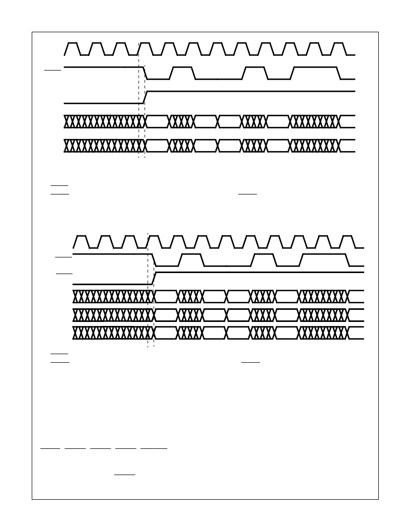
FIGURE 13. OUTPUT TIMING FOR 16-BIT YCbCr MODE (DVLD_LTC = 0, DVLD_DCYC = 1)
Y
0
Cb
0
Y
1
Cr
0
Y
2
Cb
2
Y
3
Cr
2
Y
4
Cb
4
CLK
DVALID
P15-P8
P7-P0
t
DVLD
NOTES:
18. BLANK is asserted per Figure 8.
19. DAVLID is asserted for every valid pixel during both active and blanking regions. DVALID is not a 50% duty cycle synchronous output
and will appear to jitter as the Output Sample Rate converter adjusts the output timing for various data rates and clock frequency inputs.
FIGURE 14. OUTPUT TIMING FOR 16-BIT [15-BIT] RGB MODE (DVLD_LTC = 0, DVLD_DCYC = 1)
R0
G
0
R
1
G
0
R
2
G
2
R
3
G
2
R
4
G
4
CLK
DVALID
BLANK
t
DVLD
B
0
B
1
B
2
B
3
B
4
P15-P11
[P14-P10]
P10-P5
[P9-P5]
P4-P0
HMP8116
相關PDF資料 |
PDF描述 |
|---|---|
| HMP8117 | NTSC/PAL Video Decoder |
| HMP8117CN | NTSC/PAL Video Decoder |
| HMP8154 | NTSC/PAL Encoders |
| HMP8154CN | NTSC/PAL Encoders |
| HMP8156A | NTSC/PAL Encoders |
相關代理商/技術參數 |
參數描述 |
|---|---|
| HMP8117 | 制造商:INTERSIL 制造商全稱:Intersil Corporation 功能描述:NTSC/PAL Video Decoder |
| HMP8117_07 | 制造商:INTERSIL 制造商全稱:Intersil Corporation 功能描述:NTSC/PAL Video Decoder |
| HMP8117CN | 功能描述:編碼器、解碼器、復用器和解復用器 80PQFP,0+70C NTSC/PAL VIDEO DECODER W/MA RoHS:否 制造商:Micrel 產品:Multiplexers 邏輯系列:CMOS 位數: 線路數量(輸入/輸出):2 / 12 傳播延遲時間:350 ps, 400 ps 電源電壓-最大:2.625 V, 3.6 V 電源電壓-最小:2.375 V, 3 V 最大工作溫度:+ 85 C 安裝風格:SMD/SMT 封裝 / 箱體:QFN-44 封裝:Tray |
| HMP8117CN96 | 制造商:Rochester Electronics LLC 功能描述:- Bulk |
| HMP8117CNZ | 功能描述:編碼器、解碼器、復用器和解復用器 W/ANNEAL 80PQFP 0+70 DECODER W/MA RoHS:否 制造商:Micrel 產品:Multiplexers 邏輯系列:CMOS 位數: 線路數量(輸入/輸出):2 / 12 傳播延遲時間:350 ps, 400 ps 電源電壓-最大:2.625 V, 3.6 V 電源電壓-最小:2.375 V, 3 V 最大工作溫度:+ 85 C 安裝風格:SMD/SMT 封裝 / 箱體:QFN-44 封裝:Tray |
發布緊急采購,3分鐘左右您將得到回復。