- 您現在的位置:買賣IC網 > PDF目錄385391 > HS1B-1245RH-Q (INTERSIL CORP) Radiation Hardened, Dual, High Speed, Low Power Video Operational Amplifier with Output Disable PDF資料下載
參數資料
| 型號: | HS1B-1245RH-Q |
| 廠商: | INTERSIL CORP |
| 元件分類: | 音頻/視頻放大 |
| 英文描述: | Radiation Hardened, Dual, High Speed, Low Power Video Operational Amplifier with Output Disable |
| 中文描述: | VIDEO AMPLIFIER, CDIP14 |
| 封裝: | SIDE BRAZED, CERAMIC, DIP-14 |
| 文件頁數: | 2/4頁 |
| 文件大小: | 44K |
| 代理商: | HS1B-1245RH-Q |
2
Application Information
Optimum Feedback Resistor
Although a current feedback amplifier’s bandwidth
dependency on closed loop gain isn’t as severe as that of a
voltage feedback amplifier, there can be an appreciable
decrease in bandwidth at higher gains. This decrease may
be minimized by taking advantage of the current feedback
amplifier’s unique relationship between bandwidth and R
F
.
All current feedback amplifiers require a feedback resistor,
even for unity gain applications, and R
F
, in conjunction with
the internal compensation capacitor, sets the dominant pole
of the frequency response. Thus, the amplifier’s bandwidth is
inversely proportional to R
F
. The HS-1245RH design is
optimized for a 560
R
F
at a gain of +2. Decreasing R
F
decreases stability, resulting in excessive peaking and
overshoot (Note: Capacitive feedback will cause the same
problems due to the feedback impedance decrease at higher
frequencies). At higher gains the amplifier is more stable, so
R
F
can be decreased in a trade-off of stability for bandwidth.
The table below lists recommended R
F
values for various
gains, and the expected bandwidth. For good channel-to-
channel gain matching, it is recommended that all resistors
(termination as well as gain setting) be
±
1% tolerance or better.
Note that a series input resistor, on +IN, is required for a gain of
+1, to reduce gain peaking and increase stability.
Non-Inverting Input Source Impedance
For best operation, the D.C. source impedance looking out of
the non-inverting input should be
≥
50
.
This is especially
important in inverting gain configurations where the non-
inverting input would normally be connected directly to GND.
Optional GND Pin for TTL Compatibility
The HS-1245RH derives an internal GND reference for the
digital circuitry as long as the power supplies are
symmetrical about GND. The GND reference is used to
ensure the TTL compatibility of the DISABLE inputs. With
symmetrical supplies the GND pin (Pin 12) may be floated,
or connected directly to GND. If asymmetrical supplies (e.g.
+10V, 0V) are utilized, and TTL compatibility is desired, the
GND pin must be connected to GND.
PC Board Layout
The frequency response of this amplifier depends greatly on
the amount of care taken in designing the PC board.
The
use of low inductance components such as chip
resistors and chip capacitors is strongly recommended,
while a solid ground plane is a must!
Attention should be given to decoupling the power supplies.
A large value (10
μ
F) tantalum in parallel with a small value
(0.1
μ
F) chip capacitor works well in most cases.
Terminated microstrip signal lines are recommended at the
input and output of the device. Capacitance directly on the
output must be minimized, or isolated as discussed in the
next section.
Care must also be taken to minimize the capacitance to
ground seen by the amplifier’s inverting input (-IN). The
larger this capacitance, the worse the gain peaking, resulting
in pulse overshoot and possible instability. To this end, it is
recommended that the ground plane be removed under
traces connected to -IN, and connections to -IN should be
kept as short as possible.
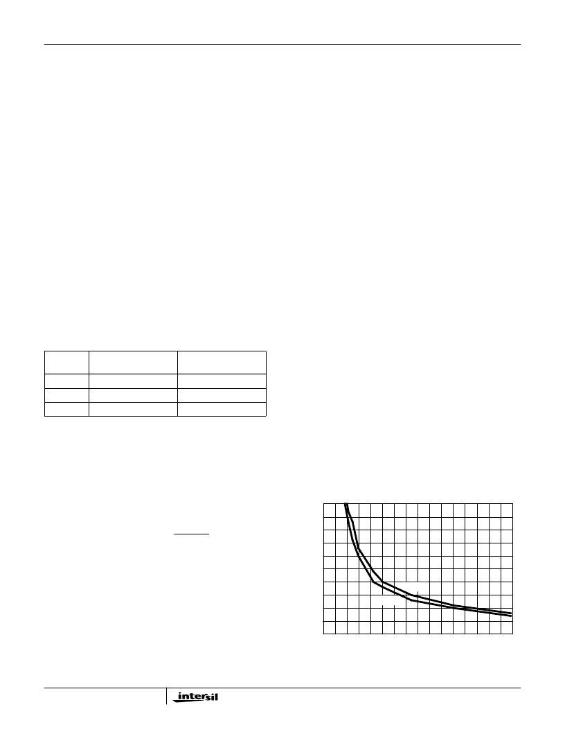
Driving Capacitive Loads
Capacitive loads, such as an A/D input, or an improperly
terminated transmission line will degrade the amplifier’s
phase margin resulting in frequency response peaking and
possible oscillations. In most cases, the oscillation can be
avoided by placing a resistor (R
S
) in series with the output
prior to the capacitance.
Figure 1 details starting points for the selection of this
resistor. The points on the curve indicate the R
S
and C
L
combinations for the optimum bandwidth, stability, and
settling time, but experimental fine tuning is recommended.
Picking a point above or to the right of the curve yields an
overdamped response, while points below or left of the curve
indicate areas of underdamped performance.
R
S
and C
L
form a low pass network at the output, thus
limiting system bandwidth well below the amplifier
bandwidth of 290MHz (for A
V
= +1). By decreasing R
S
as
C
L
increases (as illustrated in the curves), the maximum
bandwidth is obtained without sacrificing stability. Even so,
bandwidth does decrease as you move to the right along
the curve. For example, at A
V
= +1, R
S
= 62
, C
L
= 40pF,
the overall bandwidth is limited to 180MHz, and bandwidth
drops to 70MHz at A
V
= +1, R
S
= 8
, C
L
= 400pF.
GAIN
(A
CL
)
-1
R
F
(
)
510
BANDWIDTH
(MHz)
230
+1
560 (+
R
S
= 560
)
560
290
+2
530
0
100
200
300
400
0
10
20
30
40
50
LOAD CAPACITANCE (pF)
S
)
A
V
= +1
A
V
= +2
150
250
350
50
FIGURE 1. RECOMMENDED SERIES OUTPUT RESISTOR vs
LOAD CAPACITANCE
HS-1245RH
相關PDF資料 |
PDF描述 |
|---|---|
| HS-1254RH | Radiation Hardened, High Speed, Low Power Dual Operational Amplifier with Disable |
| HS9-1254RH-Q | Radiation Hardened, High Speed, Low Power Dual Operational Amplifier with Disable |
| HS9-1254RH | Radiation Hardened, High Speed, Low Power Dual Operational Amplifier with Disable |
| HS-1450 | CRYSTAL CLOCK OSCILLATORS |
| HS-A1450-FREQ | CRYSTAL CLOCK OSCILLATORS |
相關代理商/技術參數 |
參數描述 |
|---|---|
| HS1B-1412RH-Q | 制造商:INTERSIL 制造商全稱:Intersil Corporation 功能描述:Radiation Hardened, Quad, High Speed, Low Power, Video Closed Loop Buffer |
| HS1B150 | 制造商:Sola/Hevi-Duty 功能描述:DISTRIBUTION TRANSFORMER; Primary Voltages:2 x 240V; Secondary Voltages:2 x 120V; Current Rating:1.25A; Power Rating:150VA; Plug Type:-; Approval Bodies:CSA / UL; External Depth:4"; External Height:8"; External Width:4"; Series:HS1 ;RoHS Compliant: Yes |
| HS1B-2420RH/PROTO | 制造商:Intersil Corporation 功能描述:RAD HARD FAST SAMPLE AND HOLD, DIP, PROTOTYPE,CLASS V - Rail/Tube |
| HS1B-2420RH-Q | 制造商:Intersil Corporation 功能描述:SAMPLE AND HOLD 1CH 6US 14PIN SBDIP - Rail/Tube |
| HS1B250 | 制造商:Sola/Hevi-Duty 功能描述:Transformer;Single Phase;Pri:240x480V, Sec:120/240V;60Hz;0.25kVA;4In.W;8In.H 制造商:Sola/Hevi-Duty 功能描述:DISTRIBUTION TRANSFORMER 制造商:Sola/Hevi-Duty 功能描述:DISTRIBUTION TRANSFORMER; Primary Voltages:2 x 240V; Secondary Voltages:2 x 120V; Current Rating:2.08A; Power Rating:250VA; Plug Type:-; Approval Bodies:CSA / UL; External Depth:4"; External Height:8"; External Width:4"; Series:HS1 ;RoHS Compliant: Yes |
發布緊急采購,3分鐘左右您將得到回復。