- 您現在的位置:買賣IC網 > PDF目錄385404 > HT82K95E (Holtek Semiconductor Inc.) USB Multimedia Keyboard Encoder 8-Bit MCU PDF資料下載
參數資料
| 型號: | HT82K95E |
| 廠商: | Holtek Semiconductor Inc. |
| 英文描述: | USB Multimedia Keyboard Encoder 8-Bit MCU |
| 中文描述: | 的USB多媒體鍵盤編碼器8位微控制器 |
| 文件頁數: | 4/48頁 |
| 文件大小: | 319K |
| 代理商: | HT82K95E |
第1頁第2頁第3頁當前第4頁第5頁第6頁第7頁第8頁第9頁第10頁第11頁第12頁第13頁第14頁第15頁第16頁第17頁第18頁第19頁第20頁第21頁第22頁第23頁第24頁第25頁第26頁第27頁第28頁第29頁第30頁第31頁第32頁第33頁第34頁第35頁第36頁第37頁第38頁第39頁第40頁第41頁第42頁第43頁第44頁第45頁第46頁第47頁第48頁
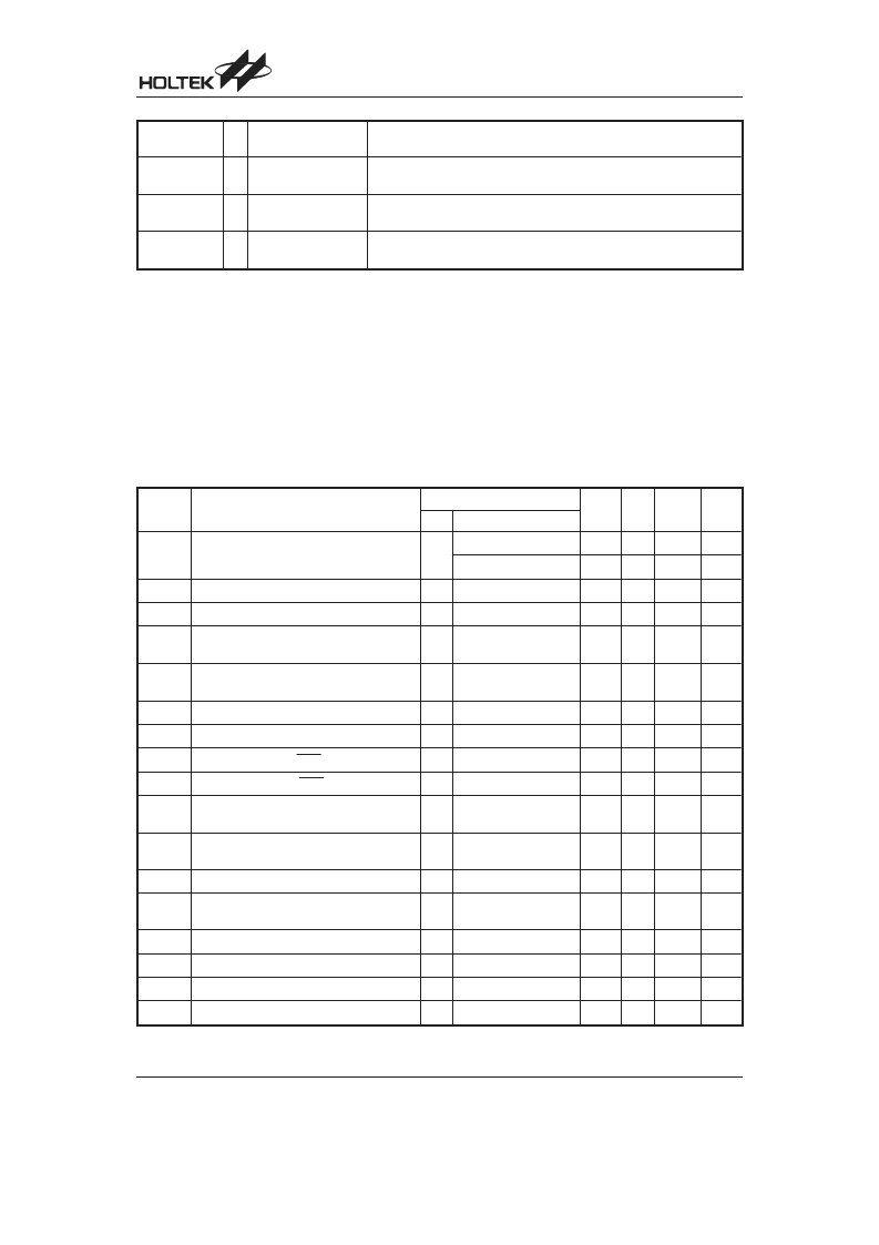
Pin Name
I/O
ROM Code
Option
Description
USBD+/CLK
I/O
USBD+ or PS2 CLK I/O line
USB or PS2 function is controlled by software control register
USBD-/DATA
I/O
USBD- or PS2 DATA I/O line
USB or PS2 function is controlled by software control register
OSC1
OSC2
I
O
OSC1, OSC2 are connected to a 6MHz or 12MHz Crystal/resonator
(determined by software instructions) for the internal system clock.
Absolute Maximum Ratings
Supply Voltage...........................V
SS
0.3V to V
SS
+6.0V
Storage Temperature............................ 50 C to 125 C
Input Voltage..............................V
SS
0.3V to V
DD
+0.3V
Operating Temperature...............................0 C to 70 C
Note: These are stress ratings only. Stresses exceeding the range specified under Absolute Maximum Ratings may
cause substantial damage to the device. Functional operation of this device at other conditions beyond those
listed in the specification is not implied and prolonged exposure to extreme conditions may affect device reliabil-
ity.
D.C. Characteristics
Ta=25 C
Symbol
Parameter
Test Conditions
Min.
Typ.
Max.
Unit
V
DD
Conditions
V
DD
Operating Voltage
f
SYS
=6MHz
4.2
5.5
V
f
SYS
=12MHz
4.2
5.5
V
I
DD1
Operating Current (6MHz Crystal)
5V
No load, f
SYS
=6MHz
6.5
12
mA
I
DD2
Operating Current (12MHz Crystal)
5V
No load, f
SYS
=12MHz
7.5
16
mA
I
STB1
Standby Current (WDT Enabled)
5V
No load, system HALT,
USB suspend
250
A
I
STB2
Standby Current (WDT Disabled)
5V
No load, system HALT,
USB suspend
230
A
V
IL1
Input Low Voltage for I/O Ports
5V
0
0.8
V
V
IH1
Input High Voltage for I/O Ports
5V
2
5
V
V
IL2
Input Low Voltage (RES)
5V
0
0.4V
DD
V
V
IH2
Input High Voltage (RES)
5V
0.9V
DD
V
DD
V
I
OL1
I/OPortSinkCurrentforPA1~PA7,PB,PC,
PD
5V
V
OL
=3.4V
10
15
20
mA
I
OL2
I/OPortSinkCurrentforPA1~PA7,PB,PC,
PD
5V
V
OL
=0.4V
2
4
8
mA
I
OL3
I/O Port Sink Current for PA0
5V
V
OL
=0.4V
7
10
13
mA
I
OH1
I/O Port Source Current for PA1~PA7, PB,
PC, PD
5V
V
OH
=3.4V
2
4
8
mA
I
OH2
I/O Port Source Current for PA0
5V
V
OH
=3.4V
12
18
24
mA
R
PH
Pull-high Resistance for PA, PB, PC, PD
5V
25
50
80
k
V
LVR
Low Voltage Reset
3
3.4
4.0
V
V
V33O
3.3V Regulator Output
5V
I
V33O
= 5mA
3.0
3.3
3.6
V
HT82K95E/HT82K95A
Rev. 1.20
4
October 24, 2005
相關PDF資料 |
PDF描述 |
|---|---|
| HT82K96A | USB Multimedia Keyboard Encoder 8-Bit Mask MCU |
| HT82K96E | 8-Bit USB Multimedia Keyboard Encoder OTP MCU |
| HT82M21A | 3-Key 3D USB+PS/2 Optical Mouse Controller |
| HT82M22 | 5-Key 3D USB+PS/2 Optical Mouse Controller |
| HT82M22A | 5-Key 3D USB+PS/2 Optical Mouse Controller |
相關代理商/技術參數 |
參數描述 |
|---|---|
| HT82K95EE | 制造商:HOLTEK 制造商全稱:Holtek Semiconductor Inc 功能描述:USB Multimedia Keyboard Encoder 8-Bit MCU |
| HT82K96A | 制造商:HOLTEK 制造商全稱:Holtek Semiconductor Inc 功能描述:USB Multimedia Keyboard Encoder 8-Bit Mask MCU |
| HT82K96E | 制造商:HOLTEK 制造商全稱:Holtek Semiconductor Inc 功能描述:8-Bit USB Multimedia Keyboard Encoder OTP MCU |
| HT82K96E_07 | 制造商:HOLTEK 制造商全稱:Holtek Semiconductor Inc 功能描述:USB Multimedia Keyboard Encoder 8-Bit OTP MCU |
| HT82M13 | 制造商:未知廠家 制造商全稱:未知廠家 功能描述:Mouse/Trackball Controller |
發布緊急采購,3分鐘左右您將得到回復。