- 您現在的位置:買賣IC網 > PDF目錄385405 > HT84XXX (Holtek Semiconductor Inc.) Magic VoiceTM PDF資料下載
參數資料
| 型號: | HT84XXX |
| 廠商: | Holtek Semiconductor Inc. |
| 英文描述: | Magic VoiceTM |
| 中文描述: | 魔術VoiceTM |
| 文件頁數: | 10/31頁 |
| 文件大小: | 246K |
| 代理商: | HT84XXX |
第1頁第2頁第3頁第4頁第5頁第6頁第7頁第8頁第9頁當前第10頁第11頁第12頁第13頁第14頁第15頁第16頁第17頁第18頁第19頁第20頁第21頁第22頁第23頁第24頁第25頁第26頁第27頁第28頁第29頁第30頁第31頁
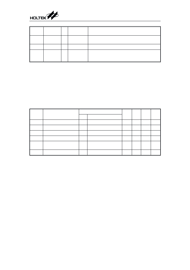
Pin No.
Pin Name I/O
Internal
Connection
Description
20~17
PA0~PA3
I
Wake-up
Pull-high
Trigger inputs
Can also be configured as wake-up inputs
21, 22
VSS
Negative power supply, ground
23
OSC
I
Built-in RC oscillator
An oscillator resistor is connected between OSC and
VSS
Absolute Maximum Ratings
Supply Voltage................................. 0.3V to 6V
Storage Temperature................. 50 C to 125 C
Input Voltage.................V
SS
0.3V to V
DD
+0.3V
Operating Temperature .............. 20 C to 70 C
Note: These are stress ratings only. Stresses exceeding the range specified under Absolute Maxi-
mumRatings maycausesubstantialdamagetothedevice.Functionaloperationofthisdevice
at other conditions beyond those listed in the specification is not implied and prolonged expo-
sure to extreme conditions may affect device reliability.
Electrical Characteristics
Ta=25 C
Symbol
Parameter
Test Conditions
Min.
Typ.
Max.
Unit
V
DD
Conditions
V
DD
Operating Voltage
2.4
5.2
V
I
STB
Standby Current
3V
No load, system HALT
1
3
A
I
DD
Operating Current
3V
No load, f
SYS
=4MHz
5
8
mA
I
OL
PB0~PB7 Sink Current
3V
V
OL
=0.3V
4
6
mA
I
O
Max. AUD1 and AUD2
Output Current
3V
V
OH
=0.6V
1.5
2
mA
f
SYS
System Frequency
3V
R
OSC
=240k
3.6
4.0
4.4
MHz
HT84XXX
10
April 26, 2000
相關PDF資料 |
PDF描述 |
|---|---|
| HT84072 | Magic VoiceTM |
| HT84144 | Magic VoiceTM |
| HT84192 | Magic VoiceTM |
| HT84384 | Magic VoiceTM |
| HT85036 | Green Voice |
相關代理商/技術參數 |
參數描述 |
|---|---|
| HT85006 | 制造商:未知廠家 制造商全稱:未知廠家 功能描述:Industrial Control IC |
| HT85009 | 制造商:未知廠家 制造商全稱:未知廠家 功能描述:Industrial Control IC |
| HT85012 | 制造商:未知廠家 制造商全稱:未知廠家 功能描述:Industrial Control IC |
| HT85018 | 制造商:未知廠家 制造商全稱:未知廠家 功能描述:Industrial Control IC |
| HT85024 | 制造商:未知廠家 制造商全稱:未知廠家 功能描述:Industrial Control IC |
發布緊急采購,3分鐘左右您將得到回復。