- 您現在的位置:買賣IC網 > PDF目錄385407 > HT93214B (Holtek Semiconductor Inc.) 1-memory Tone/Pulse Dialer PDF資料下載
參數資料
| 型號: | HT93214B |
| 廠商: | Holtek Semiconductor Inc. |
| 英文描述: | 1-memory Tone/Pulse Dialer |
| 中文描述: | 1內存音頻/脈沖撥號器 |
| 文件頁數: | 4/16頁 |
| 文件大小: | 194K |
| 代理商: | HT93214B |
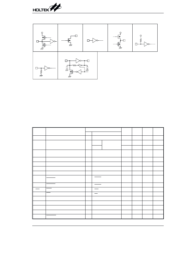
Approximate internal connection circuits
Absolute Maximum Ratings
Supply Voltage............................................ 0.3V to 6V
Storage Temperature............................ 50 C to 125 C
Input Voltage..............................V
SS
0.3V to V
DD
+0.3V
Operating Temperature........................... 20 C to 75 C
Note: These are stress ratings only. Stresses exceeding the range specified under Absolute Maximum Ratings may
cause substantial damage to the device. Functional operation of this device at other conditions beyond those
listed in the specification is not implied and prolonged exposure to extreme conditions may affect device reliabil-
ity.
Electrical Characteristics
F
OSC
=3.5795MHz, Ta=25 C
Symbol
Parameter
Test Conditions
Min.
Typ.
Max.
Unit
V
DD
Conditions
V
DD
Operating Voltage
2
5.5
V
I
DD
Operating Current
2.5V
Pulse
Off-hook
Keypad entry
0.2
1
mA
Tone
0.6
2
mA
I
STB
Standby Current
1V
On-hook, no load
No entry
1
A
V
R
Memory Retention Voltage
1
5
V
I
R
Memory Retention Current
1V
On-hook
0.1
0.2
A
V
IL
Input Low Voltage
V
SS
0.2V
DD
V
V
IH
Input High Voltage
0.8V
DD
V
DD
V
I
XMO
XMUTE Leakage Voltage
V
XMUTE
=12V
No entry
1
A
I
OLXM
XMUTE Sink Current
2.5V V
XMUTE
=0.5V
1
mA
I
HKS
HKS Pin Input Current
2.5V V
HKS
=2.5V
0.1
A
R
HFI
HFI Pull- High Resistance
2.5V V
HFI
=0V
200
k
I
OH1
Keypad Pin Source Current
2.5V V
OH
=0V
4
40
A
I
OL1
Keypad Pin Sink Current
2.5V V
OL
=2.5V
200
400
A
I
OH2
HFO Pin Source Current
2.5V V
OH
=2V
1
mA
I
OL2
HFO Pin Sink Current
2.5V V
OL
=0.5V
1
mA
I
OL3
MODEO Sink Current
2.5V V
OL
=0.5V
0.6
3.5
mA
HT93214 Series
Rev. 1.10
4
October 2, 2002
7
*
* 7 1
*
* 7
8 )
+
* 7
8
$ 9 4
* 7
) ) (
7
相關PDF資料 |
PDF描述 |
|---|---|
| HT93LC46 | 1K 3-Wire CMOS Serial EEPROM(1K CMOS 三線控制串行EEPROM) |
| HT93LC56 | 2K 3-Wire CMOS Serial EEPROM |
| HT93LC66 | 4K 3-Wire CMOS Serial EEPROM |
| HT93LC86 | CMOS 16K 3-Wire Serial EEPROM |
| HT9480 | Pager Controller |
相關代理商/技術參數 |
參數描述 |
|---|---|
| HT93214BL | 制造商:未知廠家 制造商全稱:未知廠家 功能描述:Tone/Pulse Telephone Dialer |
| HT93214BLT | 制造商:未知廠家 制造商全稱:未知廠家 功能描述:Tone/Pulse Telephone Dialer |
| HT93214BT | 制造商:未知廠家 制造商全稱:未知廠家 功能描述:Tone/Pulse Telephone Dialer |
| HT93214C | 制造商:未知廠家 制造商全稱:未知廠家 功能描述:Tone/Pulse Telephone Dialer |
| HT93214CL | 制造商:未知廠家 制造商全稱:未知廠家 功能描述:Tone/Pulse Telephone Dialer |
發布緊急采購,3分鐘左右您將得到回復。