- 您現在的位置:買賣IC網 > PDF目錄385408 > HT95CXXX (Holtek Semiconductor Inc.) CID Type Phone 8-Bit MCU PDF資料下載
參數資料
| 型號: | HT95CXXX |
| 廠商: | Holtek Semiconductor Inc. |
| 英文描述: | CID Type Phone 8-Bit MCU |
| 中文描述: | 刑事偵緝式電話8位微控制器 |
| 文件頁數: | 23/51頁 |
| 文件大小: | 384K |
| 代理商: | HT95CXXX |
第1頁第2頁第3頁第4頁第5頁第6頁第7頁第8頁第9頁第10頁第11頁第12頁第13頁第14頁第15頁第16頁第17頁第18頁第19頁第20頁第21頁第22頁當前第23頁第24頁第25頁第26頁第27頁第28頁第29頁第30頁第31頁第32頁第33頁第34頁第35頁第36頁第37頁第38頁第39頁第40頁第41頁第42頁第43頁第44頁第45頁第46頁第47頁第48頁第49頁第50頁第51頁
HT95CXXX
Rev. 1.50
23
May 26, 2005
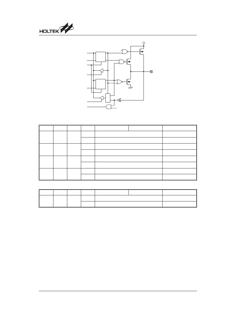
Some input/output pins can be optioned to LCD outputs by software.
Bit No.
Label
R/W
Value
400/40P
300/30P
200/20P
5
SPE0
RW
0
SEG47~SEG44
1
PE3~PE0
7
SPD1
RW
0
SEG43~SEG40
1
PD7~PD4
6
SPD0
RW
0
SEG39~SEG36
1
PD3~PD0
1
VBIAS
RW
0
COM7~COM0
COM7~COM0
1
COM7~COM0 are unavailable
PD7~PD0
LCDIO (28H) Register
Bit No.
Label
R/W
Value
400/40P
300/30P
200/20P
1
VBIAS
RW
0
COM7~COM0
COM7~COM0
1
COM7~COM0 are unavailable
PD7~PD0
LCDC (2DH) Register
6
/ / " 1
"
" .
0
"
" $ 4 )
" .
0
<
"
/ =
"
"
D
9
D 7
D
9
D 7
/ " 7
" 7
.
"
/ "
"
"
/ "
.
"
"
" 7
Input/Output Ports
When the PD0~PD7 or the PE0~PE3 are not selected,
the I/O port control register PDC(19H), PEC(1BH) could
be readable/writable and be used as a general user
RAM, but this function is not available for register PD
(18H) and PE (1AH).
FSK Decoder
The FSK decoder supports three interrupt sources to
the peripheral interrupt vector. There are ring detect or
line reversal detect, FSK carrier detect and FSK packet
data. Write 0 to the control flag, RMSK, CMSK and
FMSK will enable these interrupt. When any of these in-
terrupt occurs, its interrupt flag (RDETF, CDETF, FSKF)
will be set to 1 by hardware even if the interrupt is dis-
abled. These interrupts will cause a peripheral interrupt
if the peripheral interrupt is enabled.When the periph-
eral interrupt occurs, the interrupt request flag PERF will
be set and a subroutine call to location 10H will occur.
Returning from the interrupt subroutine, the interrupt
flag RDETF, CDETF or FSKF will not be cleared by
hardware, the user should clear it by software. If inter-
rupt flag RDETF is not cleared, next ring detect interrupt
will be inhibited, other interrupt flags CDETF, FSKF
have the same behavior. The power down mode
(F_PWDN=1) will terminate all the FSK decoder func-
tion, however, the registers FSKC, FSKS and FSKD are
accessible at this power down mode.
相關PDF資料 |
PDF描述 |
|---|---|
| HT95L400-128QFP-A | LCD Type Phone 8-Bit MCU |
| HT95L100-64QEP-A | LCD Type Phone 8-Bit MCU |
| HT95L10P-64QEP-A | LCD Type Phone 8-Bit MCU |
| HT95L100-64QFP-A | 8-Bit LCD Type Phone Controller MCU |
| HT95L10P-64QFP-A | 8-Bit LCD Type Phone Controller MCU |
相關代理商/技術參數 |
參數描述 |
|---|---|
| HT95L000 | 制造商:HOLTEK 制造商全稱:Holtek Semiconductor Inc 功能描述:CID Type Phone 8-Bit MCU |
| HT95L000-56SSOP-A | 制造商:HOLTEK 制造商全稱:Holtek Semiconductor Inc 功能描述:LCD Type Phone 8-Bit MCU |
| HT95L00P | 制造商:HOLTEK 制造商全稱:Holtek Semiconductor Inc 功能描述:LCD Type Phone 8-Bit MCU |
| HT95L00P-56SSOP-A | 制造商:HOLTEK 制造商全稱:Holtek Semiconductor Inc 功能描述:LCD Type Phone 8-Bit MCU |
| HT95L100 | 制造商:HOLTEK 制造商全稱:Holtek Semiconductor Inc 功能描述:CID Type Phone 8-Bit MCU |
發布緊急采購,3分鐘左右您將得到回復。