- 您現在的位置:買賣IC網 > PDF目錄385414 > HY27SS08121M (Hynix Semiconductor Inc.) 512Mbit (64Mx8bit / 32Mx16bit) NAND Flash PDF資料下載
參數資料
| 型號: | HY27SS08121M |
| 廠商: | Hynix Semiconductor Inc. |
| 英文描述: | 512Mbit (64Mx8bit / 32Mx16bit) NAND Flash |
| 中文描述: | 512兆(64Mx8bit / 32Mx16bit)NAND閃存 |
| 文件頁數: | 18/43頁 |
| 文件大小: | 729K |
| 代理商: | HY27SS08121M |
第1頁第2頁第3頁第4頁第5頁第6頁第7頁第8頁第9頁第10頁第11頁第12頁第13頁第14頁第15頁第16頁第17頁當前第18頁第19頁第20頁第21頁第22頁第23頁第24頁第25頁第26頁第27頁第28頁第29頁第30頁第31頁第32頁第33頁第34頁第35頁第36頁第37頁第38頁第39頁第40頁第41頁第42頁第43頁
Rev 0.6 / Oct. 2004
18
HY27SS(08/16)121M Series
HY27US(08/16)121M Series
512Mbit (64Mx8bit / 32Mx16bit) NAND Flash
Copy Back Program
The Copy Back Program operation is used to copy the data stored in one page and reprogram it in another page.
The Copy Back Program operation does not require external memory and so the operation is faster and more efficient
because the reading and loading cycles are not required. The operation is particularly useful when a portion of a block
is updated and the rest of the block needs to be copied to the newly assigned block.
If the Copy Back Program operation fails an error is signalled in the Status Register. However as the standard external
ECC cannot be used with the Copy Back operation bit error due to charge loss cannot be detected. For this reason it is
recommended to limit the number of Copy Back operations on the same data and/or to improve the performance of
the ECC.
The Copy Back Program operation requires three steps:
- 1. The source page must be read using the Read A command (one bus write cycle to setup the command and then
4 bus write cycles to input the source page address). This operation copies all 264 Words/ 528 Bytes from the page
into the Page Buffer.
- 2. When the device returns to the ready state (Ready/Busy High), the second bus write cycle of the command is
given with the 4 bus cycles to input the target page address. A25must be the same for the Source and Target Pages.
- 3. Then the confirm command is issued to start the P/E/R Controller.
After a Copy Back Program operation, a partial page program is not allowed in the target page until the block has been
erased.
See Figure 15 for an example of the Copy Back operation.
Block Erase
Erase operations are done one block at a time. An erase operation sets all of the bits in the addressed block to '1'. All
previous data in the block is lost. An erase operation consists of three steps (refer to Figure 17):
1. One bus cycle is required to setup the Block Erase command.
2. Only three bus cycles for 512Mb devices are required to input the block address. The first cycle (A0 to A7) is not
required as only addresses A14 to A25 (highest address depends on device density) are valid, A9 to A13 are ignored.
In the last address cycle I/O
0
to I/O
7
must be set to V
IL
.
3. One bus cycle is required to issue the confirm command to start the P/E/R Controller.
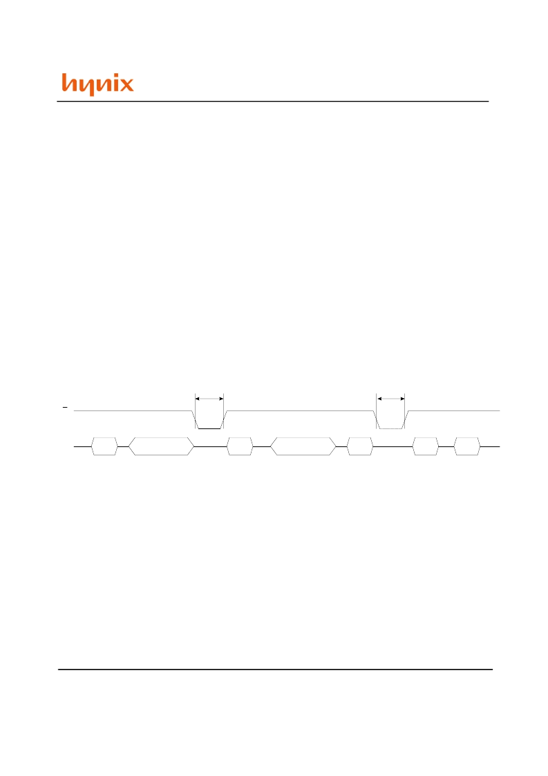
Figure 15. Copy Back Operation
Source
Address Inputs
I/O
00h
Copy Back
Code
Target
Address Inputs
8Ah
10h
70h
Read
Code
Read Status Register
SR0
Busy
tBLBH2
(Program Busy time)
tBLBH1
(Read Busy time)
RB
相關PDF資料 |
PDF描述 |
|---|---|
| HY27SS16121M | 512Mbit (64Mx8bit / 32Mx16bit) NAND Flash |
| HY27US08121M | 512Mbit (64Mx8bit / 32Mx16bit) NAND Flash |
| HY27USxxx | 512Mbit (64Mx8bit / 32Mx16bit) NAND Flash |
| HY27US16121M | 512Mbit (64Mx8bit / 32Mx16bit) NAND Flash |
| HY29F002TC-70 | 2 Megabit (256K x 8), 5 Volt-only, Flash Memory |
相關代理商/技術參數 |
參數描述 |
|---|---|
| HY27SS08561A | 制造商:HYNIX 制造商全稱:Hynix Semiconductor 功能描述:256Mbit (32Mx8bit / 16Mx16bit) NAND Flash |
| HY27SS08561M | 制造商:HYNIX 制造商全稱:Hynix Semiconductor 功能描述:256Mbit (32Mx8bit / 16Mx16bit) NAND Flash |
| HY27SS16121A | 制造商:HYNIX 制造商全稱:Hynix Semiconductor 功能描述:512Mbit (64Mx8bit / 32Mx16bit) NAND Flash |
| HY27SS16121M | 制造商:HYNIX 制造商全稱:Hynix Semiconductor 功能描述:512Mbit (64Mx8bit / 32Mx16bit) NAND Flash |
| HY27SS16561A | 制造商:HYNIX 制造商全稱:Hynix Semiconductor 功能描述:256Mbit (32Mx8bit / 16Mx16bit) NAND Flash |
發布緊急采購,3分鐘左右您將得到回復。